A calibration circuit design method for pipeline adc

A calibration circuit and assembly line technology, which is applied in the direction of analog/digital conversion calibration/test, electrical components, code conversion, etc., can solve the problems of complex implementation, slow calibration speed, and high power consumption of the calibration circuit, and achieve simplification of the calibration circuit. Small power consumption and area, easy to use

Active Publication Date: 2019-03-01
UNIV OF ELECTRONICS SCI & TECH OF CHINA
View PDF4 Cites 0 Cited by
  • Summary
  • Abstract
  • Description
  • Claims
  • Application Information

AI Technical Summary

Problems solved by technology

[0005] At present, the present invention proposes a calibration circuit design with low power consumption, on-chip integration (SoC) and programmable calibration coefficients in order to solve the problems of too much power consumption, too complicated implementation and too slow calibration speed of the above-mentioned existing calibration circuit method

Method used


Image

  • A calibration circuit design method for pipeline adc
  • A calibration circuit design method for pipeline adc
  • A calibration circuit design method for pipeline adc

Examples


Embodiment Construction

[0026] The present invention is described in detail below in conjunction with accompanying drawing

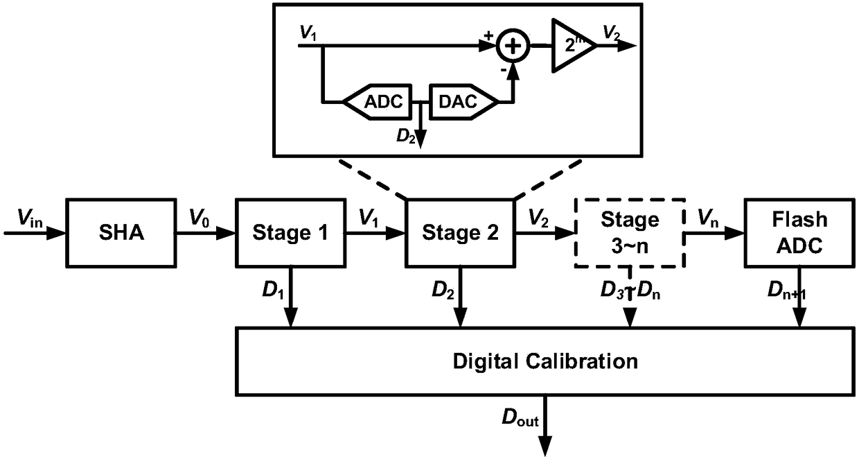
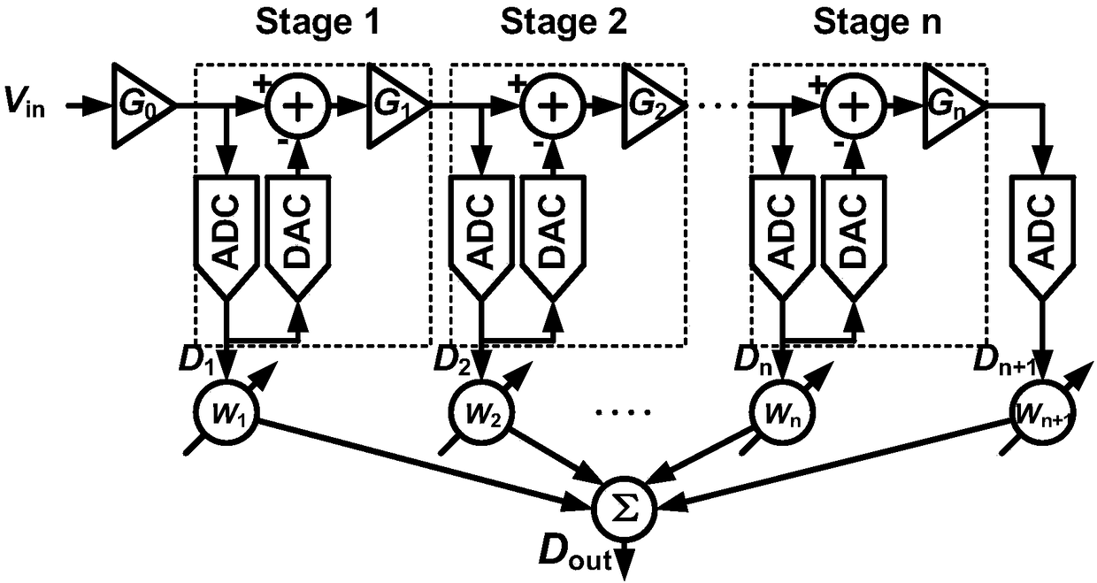
[0027] A typical pipeline ADC with a digital calibration module such as figure 1 and figure 2 Shown, including the front-end sampling and holding amplifier (SHA), sub-stage (Sub-Stage), the last stage Flash ADC and digital calibration part. The input voltage to the ADC can be expressed as,

[0028]

[0029] Among them, n is the number of stages of the pipeline ADC, G i is the redundancy gain (inter-stage gain) of the i-th redundant amplifier, G 0 Indicates the voltage gain of SHA, D n+1 Indicates the digital output of the flash ADC, V ref is the reference voltage of the entire ADC (the full-scale input of the entire ADC is -V ref ~+V ref ), V noise,out,i is the output noise voltage value of the i-th stage, D i is the i-th digital output, W i is the weight of the i-th digital output,

[0030] After adding the calibration algorithm, the equivalent voltage of the di...


PUM


Abstract

The invention relates to the technical field of analog integrated circuits, in particular to a calibration circuit design method for pipeline ADCs. The present invention mainly includes: establishing a pipelined ADC behavior level model, constructing the quantitative relationship between ADC analog circuit design parameters and digital calibration circuit design parameters and ADC performance; obtaining analog circuit design parameters and digital calibration circuit design that minimize ADC power consumption parameters; design the circuit according to the obtained parameters; obtain the calibration coefficient through the calibration algorithm and the reference DAC; write the calibration coefficient into the digital calibration circuit. The beneficial effect of the present invention is that the calibration circuit is greatly simplified, and all of them are implemented on-chip, so the power consumption and area are extremely small, compared with the traditional on-chip background calibration circuit, the power consumption and area are saved by more than 50%; the calibration circuit only increases the ADC core 10% of the area and 5% of the power consumption, so basically no additional chip area and power consumption; at the same time, the calibration system can be adjusted to adapt to different working environments.

Description

technical field [0001] The invention relates to the technical field of analog integrated circuits, in particular to a calibration circuit design method for pipeline ADCs. Background technique [0002] ADC converts analog signals into digital signals, and is widely used in various electronic systems such as communication, signal processing, and storage, and plays an irreplaceable role. At present, with the rapid development of electronic information technology, the market urgently needs high-speed, high-precision, low-voltage and low-power ADCs that can be integrated with digital circuits. Pipeline ADC has become the focus and hotspot of research at home and abroad because of the good compromise between speed, precision and power consumption. [0003] The conversion accuracy of the pipeline ADC is affected by many errors in the circuit, mainly including: thermal noise, clock jitter, switch on-resistance non-linearity, capacitance mismatch, operational amplifier (hereinafter ...

Claims


Application Information

Patent Timeline
Patent Type & Authority Patents(China)
IPC IPC(8): H03M1/10
CPCH03M1/1004H03M1/1061
Inventor 唐鹤陈锐朱金粦傅晓锦
Owner UNIV OF ELECTRONICS SCI & TECH OF CHINA
Why Eureka
Try Eureka