
Preparation technology of silicon micro wire array

A preparation process and technology of micro-wires, applied in the fields of nanotechnology, nanotechnology, semiconductor/solid-state device manufacturing, etc., can solve the problem of high surface defect density, silicon micro-wire spacing, small aspect ratio, limiting the application of silicon micro-nano structures and other problems, to achieve the effect of large aspect ratio and good adhesion

Active Publication Date: 2016-07-20
SUZHOU UNIV
View PDF5 Cites 24 Cited by
  • Summary
  • Abstract
  • Description
  • Claims
  • Application Information

AI Technical Summary

Problems solved by technology

The above two situations are problems that will occur in the current process, resulting in the inability to continue the etching process.
[0007] At present, the spacing and aspect ratio of silicon microwires prepared by these technologies are relatively small (most of the spacing is 2 μm) and large aspect ratio (>15 ) There are still difficulties in the preparation of silicon micro-wires, which limits the application of silicon micro-nanostructures
As mentioned above, the gap between silicon wires is too small: (1) the outer coating layer of silicon wires is difficult to penetrate to the bottom of silicon wires; (2) the density of surface defects is too large, and the carrier collection efficiency is low in the field of photoelectric conversion

Method used


Image

  • Preparation technology of silicon micro wire array
  • Preparation technology of silicon micro wire array
  • Preparation technology of silicon micro wire array

Examples


Embodiment 1

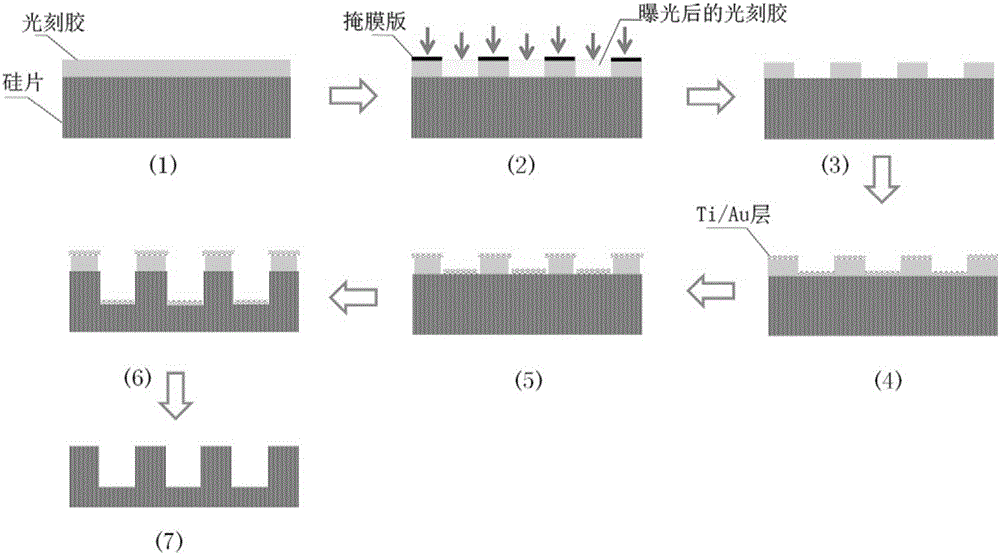
[0050] (1) Dry silicon wafers that have been ultrasonically cleaned with acetone, ethanol, and deionized water; drop RZJ304 photoresist, rotate at 5000rpm for 40 seconds, and then bake on a 100°C hot plate for 100 seconds;

[0051] (2) Press the photolithographic mask plate on the silicon wafer coated with photoresist in a soft contact method, and expose it to ultraviolet light for 8 seconds; wherein, the light-shielding area in the photolithographic plate is a square array of dots, with a diameter of 4 μm and a periodicity 8 μm in length;

[0052] (3) Develop in RZX-3038 developer for 30 seconds, take out and dry; obtain a photoresist cylinder array with a period of 8 μm and a diameter, diameter and interval of 4 μm;

[0053] (4) 5nm Ti and 40nm Au were deposited successively by electron beam evaporation technology, and the deposition rates were respectively and

[0054] (5) Soak in acetone and shake slightly for 1 minute;

[0055] (6) Configure HF and H 2 o 2 Mix the...

Embodiment 2

[0059] (1) Dry the silicon wafers that have been ultrasonically cleaned with acetone, ethanol and deionized water respectively. Drop RZJ304 photoresist, rotate at 5000rpm for 40 seconds, and then bake on a 100°C hot plate for 100 seconds;

[0060] (2) Press the photolithographic mask plate on the silicon wafer coated with photoresist in a soft contact method, and expose it to ultraviolet light for 8 seconds; wherein, the light-shielding area in the photolithographic plate is a square array of dots, with a diameter of 3 μm and a periodicity 8 μm in length;

[0061] (3) Develop in RZX-3038 developer solution for 30 seconds, take out and dry; obtain a photoresist cylinder array with a period of 8 μm, a diameter of 3 μm, and an interval of 5 μm;

[0062] (4) 5nm Ti and 40nm Au were deposited successively by electron beam evaporation technology, and the deposition rates were respectively and

[0063] (5) Soak in acetone and shake slightly for 1 minute;

[0064] (6) Configure...


PUM


Abstract

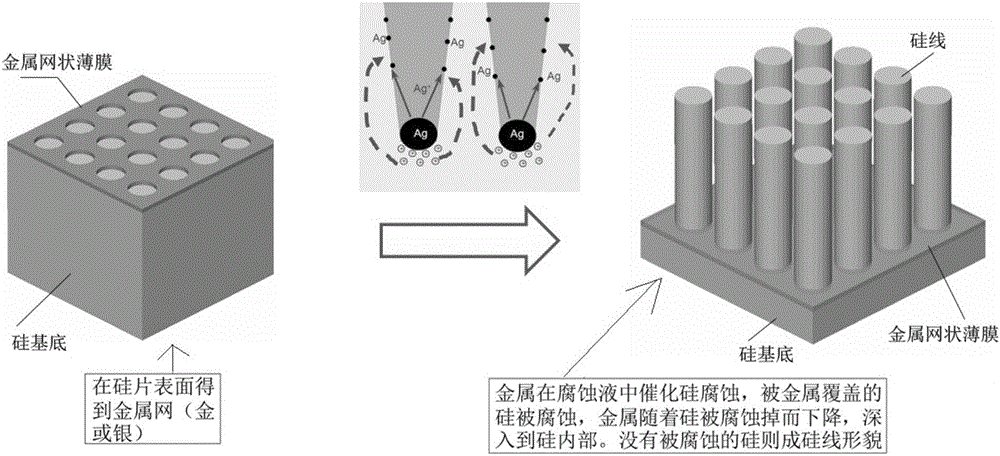
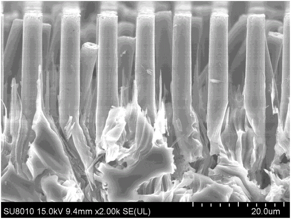
The invention discloses a preparation technology of a silicon micro wire array. The technology comprises the following steps that 1) the surface of a silicon wafer which is cleaned by washing is spin-coated with a photoresist resisting etching of a hydrofluoric acid; 2) an UV exposure technology is used to expose the silicon wafer obtained in the step 1); 3) the silicon wafer obtained in the step 2) is developed; 4) a Ti film and an Au film are deposited successively in a physical deposition method by taking the silicon wafer obtained in the step 3) as a substrate; 5) the silicon wafer obtained in the step 4) is immersed into an acetone solution and shaken for 1-3 min, the photoresist is removed incompletely, the size of the photoresist is reduced, and it is ensured that part of the bottom surface of the silicon substrate is not covered by the photoresist or metal completely; 6) the silicon wafer obtained in the step 5) is immersed into an HF and H2O2 mixed aqueous solution, and processed in an enclosed manner for 6-24 hours in the low-temperature environment of 3-15 DEG C; and 7) the photoresist and metal are removed from the silicon wafer obtained in the step 6). According to the preparation technology, the silicon micro wire array of large spacing and large length-to-diameter ratio can be obtained, and problems in the prior art are solved.

Description

technical field [0001] The invention relates to the field of micro-nano processing and manufacturing, in particular to a preparation process of a silicon micron line array with a large pitch and a large aspect ratio. Background technique [0002] In recent years, the manufacturing and controllable growth technologies of micro-nano structures have developed rapidly to develop prototype devices and industrial products with better performance, more functions and lower prices. Among them, silicon micro-nanowires have attracted much attention in the fields of photocatalysis, photoelectric conversion, and energy due to the special status of silicon materials, large aspect ratio, ultra-high specific surface area, and the ability to separate the photon incident direction from the carrier collection direction. In general, the preparation methods of silicon micro-nanowires can be divided into two categories: bottom-up method and top-down method. The bottom-up method is to obtain sili...

Claims


Application Information

Patent Timeline
IPC IPC(8): H01L21/306H01L21/027B82Y30/00B82Y40/00
CPCB82Y30/00B82Y40/00H01L21/0273H01L21/30604
Inventor 吴绍龙严继木李孝峰翟雄飞高翔
Owner SUZHOU UNIV
Learn More