
A kind of room temperature ferromagnetic magnetic semiconductor material and its application

A magnetic semiconductor and ferromagnetic technology, applied in the field of spintronics, can solve problems such as restricting the working environment, and achieve the effects of low cost, simple preparation method, and easy realization

Active Publication Date: 2018-12-14
KUNMING UNIV OF SCI & TECH
View PDF3 Cites 0 Cited by
  • Summary
  • Abstract
  • Description
  • Claims
  • Application Information

AI Technical Summary

Problems solved by technology

However, only a few magnetic semiconductor materials have room temperature ferromagnetism, which greatly limits the working environment, so the research and development of room temperature ferromagnetic magnetic semiconductor materials is imminent

Method used


Image

  • A kind of room temperature ferromagnetic magnetic semiconductor material and its application
  • A kind of room temperature ferromagnetic magnetic semiconductor material and its application
  • A kind of room temperature ferromagnetic magnetic semiconductor material and its application

Examples


Embodiment 1

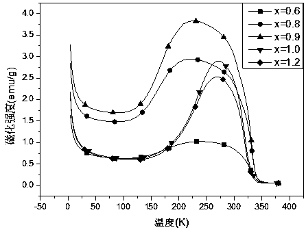
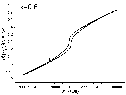
[0021] In this example, the components are Sr 3.4 Yb 0.6 co 4 o 10.5 Polycrystalline, ferromagnetic, with a Curie temperature of 328K (see figure 1 , 2), semiconductor power transmission behavior (see Figure 7 ).

Embodiment 2

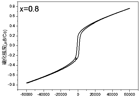
[0023] In this example, the components are Sr 3.2 Yb 0.8 co 4 o 10.5 Polycrystalline, ferromagnetic, with a Curie temperature of 331K (see figure 1 , 3), semiconductor power transmission behavior (see Figure 8 ).

Embodiment 3

[0025] In this example, the components are Sr 3.1 Yb 0.9 co 4 o 10.5 Polycrystalline, ferromagnetic, with a Curie temperature of 332K (see figure 1 , 4), semiconductor power transmission behavior (see Figure 9 ).


PUM

PropertyMeasurementUnit
Curie pointaaaaaaaaaa

Abstract

The invention discloses a novel room-temperature ferromagnetic semiconductor material and application thereof. The chemical formula of the material is Sr<4-x>YbxCo4O10.5 (x is more than or equal to 0.6 and less than or equal to 1.2), wherein the Curie temperature Tc is approximately equal to 320K-335K. A traditional solid reaction method is utilized for preparing at 1180 DEG C for 24 hours so as to obtain Sr<4-x>YbxCo4O10.5 (x is more than or equal to 0.6 and less than or equal to 1.2). The material can be applied to the fields of spin field effect transistors, spin light-emitting diodes, nonvolatile memories and the like.

Description

technical field [0001] The invention discloses a room temperature ferromagnetic semiconductor material and its application, belonging to the field of spin electronics. Background technique [0002] The contemporary and future society is dominated by information, and the processing, transmission and storage of information will require unprecedented scale and speed. Large-scale integrated circuits and high-frequency devices supported by semiconductor materials play an important role in information processing and transmission. With the development of the semiconductor industry to this day, the number of components on VLSI chips continues to increase according to Moore's law, and is approaching its limit. With the continuous shrinking of the size of a single transistor, its channel length has been developed from the previous micron level to the nanometer level, which will not only bring new problems such as increased leakage current, increased heat generation, and parasitic cap...

Claims


Application Information

Patent Timeline
Patent Type & Authority Patents(China)
IPC IPC(8): H01F1/40H01L33/26H01L29/66H01L27/10
CPCH01F1/40H01L27/10H01L29/66H01L33/26
Inventor 虞澜康冶宋世金樊堃胡建立谭红琳
Owner KUNMING UNIV OF SCI & TECH
Learn More