Method for preparing nanocrystalline diamond film by using helicon wave plasma technology

A nanocrystalline diamond and plasma technology, which is applied in metal material coating process, coating, gaseous chemical plating, etc., can solve the problems of easy pollution, filament performance attenuation, and low deposition rate of hot filament CVD

Active Publication Date: 2018-09-25
SUZHOU UNIV
View PDF8 Cites 1 Cited by
  • Summary
  • Abstract
  • Description
  • Claims
  • Application Information

AI Technical Summary

Problems solved by technology

However, they all have some disadvantages, including: microwave plasma CVD equipment is expensive, and the deposition chamber design needs to be simulated; the deposition rate of hot wire CVD is low, and the performance of the filament decays during the deposition process; the process parameters of DC arc plasma jet CVD Difficult to control, easy to pollute electrodes

Method used


Image

  • Method for preparing nanocrystalline diamond film by using helicon wave plasma technology
  • Method for preparing nanocrystalline diamond film by using helicon wave plasma technology
  • Method for preparing nanocrystalline diamond film by using helicon wave plasma technology

Examples


Embodiment Construction

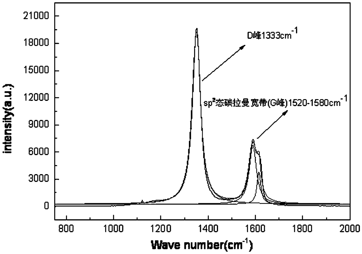
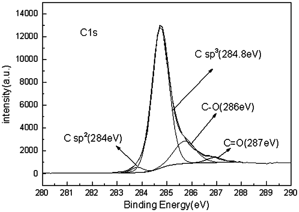
[0025] The present invention will now be further described in detail in conjunction with the accompanying drawings and embodiments. These drawings are all simplified schematic diagrams, only illustrating the basic structure of the present invention in a schematic manner, so it only shows the composition related to the present invention.

[0026] The helicon wave plasma technique adopted in the present invention prepares the method for nanocrystalline diamond film, comprises the steps:

[0027] (1) Use single crystal Si with a crystal orientation of as the substrate, and use industrial standard wet cleaning to remove the natural oxide layer and various sticky dirt on the Si surface. Put the cleaned Si substrate on the substrate table and fix it, then pump the discharge chamber to the background vacuum. After being evacuated to the background vacuum, the Ar gas and H 2 The gas is passed into the discharge chamber, and in the axial magnetic field environment, Ar and H are reali...


PUM

PropertyMeasurementUnit
strengthaaaaaaaaaa

Abstract

The invention relates to a method for preparing a nanocrystalline diamond film by adopting a helicon wave plasma technology. The method comprises the following steps: (1) introducing Ar gas and H2 gas into a discharge chamber, realizing Ar and H2 mixed gas discharge through radio frequency modulated helicon wave plasma in an axial magnetic field environment, and cleaning a substrate holder and a Si substrate; (2) closing H2 gas, introducing Ar gas and CH4 gas, and forming a nanocrystalline diamond film on the Si substrate through the radio frequency modulated helicon wave plasma in the axial magnetic field environment; and (3) cleaning the CH4 gas adsorbed to the surface of the nanocrystalline diamond film. According to the invention, the nanocrystalline diamond film is successfully prepared by the helicon wave plasma technology, the used equipment is simple, the industrial production is easy to realize, the deposition speed is high, and the problem that the filament performance is degraded is solved; moreover, the process steps are simple, and the process parameters are easy to control.

Description

technical field [0001] The invention relates to a method for preparing a nanocrystalline diamond film, in particular to a method for preparing a nanocrystalline diamond film by adopting a helicon wave plasma technology. Background technique [0002] Diamond is the substance with the most compact arrangement of atoms. Its crystal structure determines that it has many excellent physical and chemical properties, such as: extremely high hardness and elastic modulus, very low thermal expansion coefficient, high fracture strength, large Bandgap width, extremely low dielectric constant, etc. Nanocrystalline diamond (NCD) film generally refers to a diamond film with an average grain size below 100 nm. Due to the size effect, nanocrystalline diamond also exhibits many unique physical and chemical properties. For example: In addition to having many of the excellent physical and chemical properties of diamond mentioned above, nanocrystalline diamond also has higher optical transmitta...

Claims


Application Information

Patent Timeline
Patent Type & Authority Patents(China)
IPC IPC(8): C23C16/27C23C16/505
CPCC23C16/272C23C16/279C23C16/505
Inventor 吴雪梅於俊金成刚黄天源季佩宇杨佳奇诸葛兰剑
Owner SUZHOU UNIV
Why Eureka
Try Eureka