
Solution process electron transporting layer for polymer light emitting diode

An electron transport layer, light-emitting diode technology, applied in circuits, electrical components, electro-solid devices, etc., can solve problems such as PLED unsatisfactory

Inactive Publication Date: 2016-07-06
NANO & ADVANCED MATERIALS INST
View PDF3 Cites 6 Cited by
  • Summary
  • Abstract
  • Description
  • Claims
  • Application Information

AI Technical Summary

Problems solved by technology

[0005] Therefore, there remains an unmet need to fabricate PLEDs with time-saving and cost-effective manufacturing methods

Method used


Image

  • Solution process electron transporting layer for polymer light emitting diode
  • Solution process electron transporting layer for polymer light emitting diode
  • Solution process electron transporting layer for polymer light emitting diode

Examples


example 1

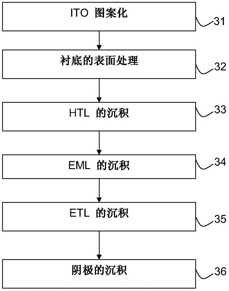
[0036] Blue PLEDs fabricated according to embodiments of the present invention. The blue PLED consists of ITO / MoO 3 (10nm) / Blue EML: Multilayer structure of 10% FIrPIc(25nm) / TPBi(10nm) / Al(150nm) in PVK. The TPBi of the ETL layer was deposited by spin coating and annealed at a temperature of 100 °C for 10 minutes. Figure 4A Brightness curves of blue PLEDs at different voltages are shown. The brightness of the blue LED is plotted against voltage. The maximum brightness of the blue PLED is 892.5cd / m 2 .

example 2

[0038] Green PLEDs fabricated according to embodiments of the present invention. The green PLED includes ITO / MoO 3 (10nm) / Green EML: 10% Ir(ppy) in PVK 3(25nm) / TPBi(10nm) / Al(150nm) multilayer structure. The TPBi of the ETL layer was deposited by spin coating and annealed at a temperature of 100 °C for 10 minutes. Figure 4B Brightness curves of green PLEDs at different voltages are shown. The brightness of the green LED is plotted against voltage. The maximum brightness of the green PLED is 1564.8cd / m 2 .

example 3

[0040] A red PLED fabricated according to an embodiment of the invention. The red PLED consists of ITO / MoO 3 (10nm) / red EML: 10% hex-Ir(piq) in PVK 3 (25nm) / TPBi(10nm) / Al(150nm) multilayer structure. The TPBi of the ETL layer was deposited by spin coating and annealed at a temperature of 100 °C for 10 minutes. Figure 4C Displays the brightness curve of the red PLED at different voltages. The brightness of a red LED is plotted against voltage. The maximum brightness of the red PLED is about 640cd / m 2 .


PUM


Abstract

The present invention relates to a method for fabricating a solution-processed PLED including an electron transport layer. The electron transport layer, deposited on an emission layer by a solution process, provides the performance comparable to those processed by vacuum deposition. In addition, the method of the present invention is able to lower manufacturing cost and reduce time for fabrication.

Description

technical field [0001] The invention relates to a polymer light-emitting diode. More specifically, the present invention relates to a method for fabricating polymer light emitting diodes by depositing a thin electron transport layer (ETL) in a solution process. Background technique [0002] Recently, the development of polymer light-emitting diodes (PLEDs) has focused on improving device efficiency and operating lifetime through multilayer device structures. In multilayer PLEDs, the electron transport layer (ETL) plays an important role in providing efficient electron transport, lowering the potential barrier between the emissive layer (EML) and the cathode, and preventing the cathode quenching effect by blocking holes. [0003] Additionally, without ETL, devices require low work function or unstable cathodes such as Ca, Ba, or CsF / Al. This is one reason why the lifetime of PLEDs is shorter than that of small molecule organic light-emitting diodes. The LiF / Al cathodes com...

Claims


Application Information

Patent Timeline
Patent Type & Authority Applications(China)
IPC IPC(8): H01L51/52H01L51/56H10K99/00
CPCH10K71/12H10K71/40H10K85/6572H10K50/16Y02E10/549H10K71/00
Inventor 蔡峥鸣卢子翘何国强
Owner NANO & ADVANCED MATERIALS INST
Learn More