Formation method of semiconductor structure

A semiconductor and gas technology, applied in semiconductor/solid-state device manufacturing, electrical components, circuits, etc., can solve the problems of holes and low density, and achieve the effect of improving density and preventing holes

Active Publication Date: 2018-12-21
SEMICON MFG INT (SHANGHAI) CORP
View PDF5 Cites 0 Cited by
  • Summary
  • Abstract
  • Description
  • Claims
  • Application Information

AI Technical Summary

Problems solved by technology

[0009] However, the existing shallow trench isolation structure has the problems of low density and holes

Method used


Image

  • Formation method of semiconductor structure
  • Formation method of semiconductor structure
  • Formation method of semiconductor structure

Examples


Embodiment Construction

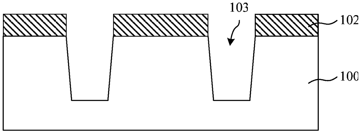
[0029] As mentioned in the background art, the shallow trench isolation structure formed in the prior art has the problems of low density and holes.

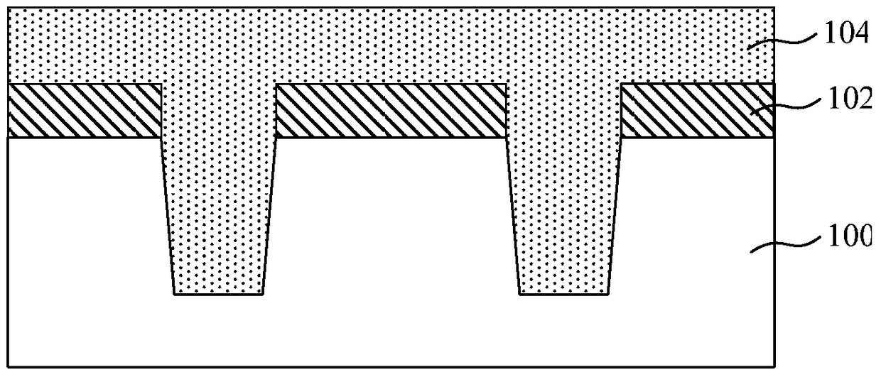
[0030] The study found that the middle area of ​​the isolation material layer formed by the high aspect ratio deposition process has low density, so the middle area of ​​the shallow trench isolation structure formed by the chemical mechanical polishing process on the isolation material layer is prone to holes or depressions, which affects the Electrical isolation performance of shallow trench isolation structures.

[0031] Further research found that the gas used in the high aspect ratio deposition process is TEOS (tetraethoxysilane, Si(OC 2 h 5 ) 4 ) and O 3 , when forming the isolation material layer, the reaction chamber maintains a certain chamber pressure and temperature, and TEOS and O 3 into the reaction chamber, TEOS and O 3 The reaction forms a silicon oxide isolation material layer. The isolation material layer is...


PUM


Abstract

The invention provides a formation method of a semiconductor structure. The formation method of a semiconductor structure comprises the steps: providing a semiconductor substrate, wherein a plurality of grooves are formed in the semiconductor substrate; forming a first oxygen ambient silica layer on the surface of the side wall and the bottom of the grooves and on the surface of the semiconductor structure, wherein part of silicon atoms on the surface of the first oxygen ambient silica layer are connected with ethoxy; performing an inertia plasma processing technology to realize bond rupture between the ethyl and oxygen atoms in the ethoxy on the surface of the first oxygen ambient silica layer to form a silicon oxygen dangling bond; performing a water vapour processing technology to realize combination of the oxygen and the hydrogen in the silicon oxygen dangling bond on the surface of the first oxygen ambient silica layer to form a silicon oxygen hydrogen bond; performing an ultraviolet processing technology to remove the protium in the silicon oxygen hydrogen bond on the surface of the first oxygen ambient silica layer to form a silicon oxygen silicon bond; performing a second high aspect ratio deposition technology to form a second oxygen ambient silica layer on the surface of the first oxygen ambient silica layer; and removing the first oxygen ambient silica layer and the second oxygen ambient silica layer on the semiconductor substrate, and forming a shallow groove isolation structure in the grooves. The formation method of a semiconductor structure can increase the compactness of the shallow groove isolation structure.

Description

technical field [0001] The invention relates to the field of semiconductor manufacturing, in particular to a method for forming a semiconductor structure. Background technique [0002] The development direction of semiconductor integrated circuits is to increase density and shrink components. In the manufacture of integrated circuits, the isolation structure is an important technology, and the components formed on the silicon substrate use the isolation structure to isolate each other. With the advancement of semiconductor manufacturing technology, shallow trench isolation (Shallow Trench Isolation, STI) technology has gradually replaced other isolation methods such as local oxidation of silicon (LOCOS) used in traditional semiconductor device manufacturing and has become a commonly used isolation structure. . [0003] With the continuous reduction of the feature size of semiconductor devices, the high aspect ratio deposition process is more and more widely used in the man...

Claims


Application Information

Patent Timeline
Patent Type & Authority Patents(China)
IPC IPC(8): H01L21/762
Inventor 邓浩徐建华肖莉红
Owner SEMICON MFG INT (SHANGHAI) CORP
Why Eureka
Try Eureka