Method for preparing high aspect ratio silicon microstructure on basis of deep reactive ion etching technology

A deep reaction ion, high aspect ratio technology, applied in the manufacture of microstructure devices, microstructure technology, microstructure devices, etc., can solve the problems of low roughness and difficulty in maintaining verticality, and achieve high instantaneous power and low The roughness of the side wall meets the effect of miniaturization

Inactive Publication Date: 2016-05-25
苏州工业园区纳米产业技术研究院有限公司
View PDF4 Cites 7 Cited by
  • Summary
  • Abstract
  • Description
  • Claims
  • Application Information

AI Technical Summary

Problems solved by technology

At present, domestic photoresist / SiO 2 There are few studies on the etching of high aspect ratio silicon structures (aspect ratio above 50:1) by composite mask, and it is difficult to maintain verticality and low roughness

Method used


Image

  • Method for preparing high aspect ratio silicon microstructure on basis of deep reactive ion etching technology

Examples


Embodiment

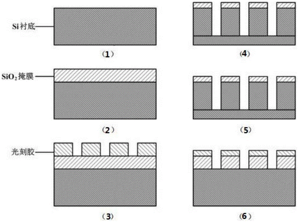
[0030] Embodiment: A method for preparing a high aspect ratio silicon microstructure based on deep reactive ion etching technology, comprising the following steps:

[0031] (1) cleaning a piece of n-type, (100) single crystal silicon as the substrate;

[0032] (2) Deposit a layer of SiO with a certain thickness on the surface of the silicon substrate 2 membrane;

[0033] (3) on SiO 2 The surface of the film is spin-coated with a certain thickness of photoresist, and the pattern transfer is realized through the photolithography process;

[0034] (4) Using reactive ion etching (RIE) etching technology, by adjusting CHF 3 and CF 4 Gas flow and etching power, the photoresist pattern is accurately copied to SiO 2 film, making SiO 2 The verticality of the membrane side wall can reach about 85 degrees;

[0035] (5) Use DRIE process to etch to form a three-dimensional deep groove structure with high aspect ratio: select a certain flow rate of SF 6 As the etching gas, select a ...


PUM

PropertyMeasurementUnit
Thicknessaaaaaaaaaa
Thicknessaaaaaaaaaa

Abstract

The invention discloses a method for preparing a high aspect ratio silicon microstructure on the basis of a deep reactive ion etching technology. The method adopts a photoresist / SiO2 composite mask to achieve high perpendicularity, low roughness etching and accurate pattern transfer of the high aspect ratio structure, and a high aspect ratio of the high aspect ratio silicon microstructure prepared by the method can reach over 100:1. By controlling etching parameters of gas flow, an etching and passivation time ratio, etching power and the like, processing on the high aspect ratio three-dimensional silicon microstructure is achieved. The method solves the technical difficult problems of small surface area, poor side wall perpendicularity, serious drill etching phenomenon, high surface roughness and the like. The three-dimensional silicon microstructure has the characteristics of large capacity-volume ratio, high reliability and the like, is very suitable for MEMS (Micro Electro Mechanical System) energy storage devices, and meets the development requirements for microminiaturization, intelligence and integration of an energy system.

Description

technical field [0001] The invention relates to a method for preparing a silicon microstructure, in particular to a method for preparing a silicon microstructure with a high aspect ratio based on a deep reactive ion etching technique. Background technique [0002] With the continuous development of micro-electromechanical systems (MicroElectroMechanicalSystem, MEMS), various functional devices such as sensors and micro-actuators are emerging, and the demand for small-sized, high-power, and highly integrated micro-energy devices has become increasingly prominent. Due to the advantages of stable structure, rapid and accurate action, high energy storage density and mass production, micro-energy devices have attracted much attention in the field of modern energy storage. [0003] Due to the limited two-dimensional area of ​​the micro-energy device structure, which cannot meet its energy storage requirements, the three-dimensional structure has gradually become a research hotspot...

Claims


Application Information

Patent Timeline
IPC IPC(8): B81C1/00
CPCB81C1/00531B81C1/00396B81C1/00619B81C1/00857
Inventor 陈婷婷
Owner 苏州工业园区纳米产业技术研究院有限公司
Why Eureka
Try Eureka