Gate-commutated thyristor with double p-base gate-cathode structure and preparation method thereof

A gate commutation, thyristor technology, applied in the direction of thyristor, semiconductor/solid-state device manufacturing, electrical components, etc., can solve the problem that the doping concentration of the p+ short base region cannot be too high, reduce the turn-off capability of the GCT chip, and increase the GCT chip. Process difficulty and other problems, to achieve the effect of eliminating the digging process, increasing the voltage, improving reliability and yield

Active Publication Date: 2018-05-29
TSINGHUA UNIV
View PDF4 Cites 2 Cited by
  • Summary
  • Abstract
  • Description
  • Claims
  • Application Information

AI Technical Summary

Problems solved by technology

[0019] 2) The doping concentration of the p+ short base region cannot be too high, because the J3 junction formed with n+, too high a concentration will lead to a lower breakdown voltage. Once the J3 junction reversely breaks down, the commutation will fail, and the GCT chip will damage
The "grooving" process makes the surface structure of the silicon wafer uneven, which greatly increases the difficulty of the follow-up process of the GCT chip, such as steaming the aluminum electrode, engraving the aluminum and other steps, which affects the consistency of the process, thereby reducing the shutdown of the GCT chip ability

Method used


Image

  • Gate-commutated thyristor with double p-base gate-cathode structure and preparation method thereof
  • Gate-commutated thyristor with double p-base gate-cathode structure and preparation method thereof
  • Gate-commutated thyristor with double p-base gate-cathode structure and preparation method thereof

Examples


Embodiment Construction

[0061] A GCT chip with a novel gate-cathode structure proposed by the present invention will be described in detail below in conjunction with the accompanying drawings and embodiments:

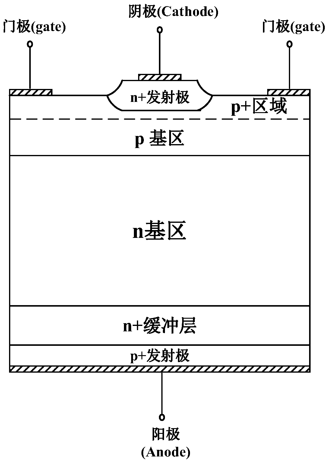
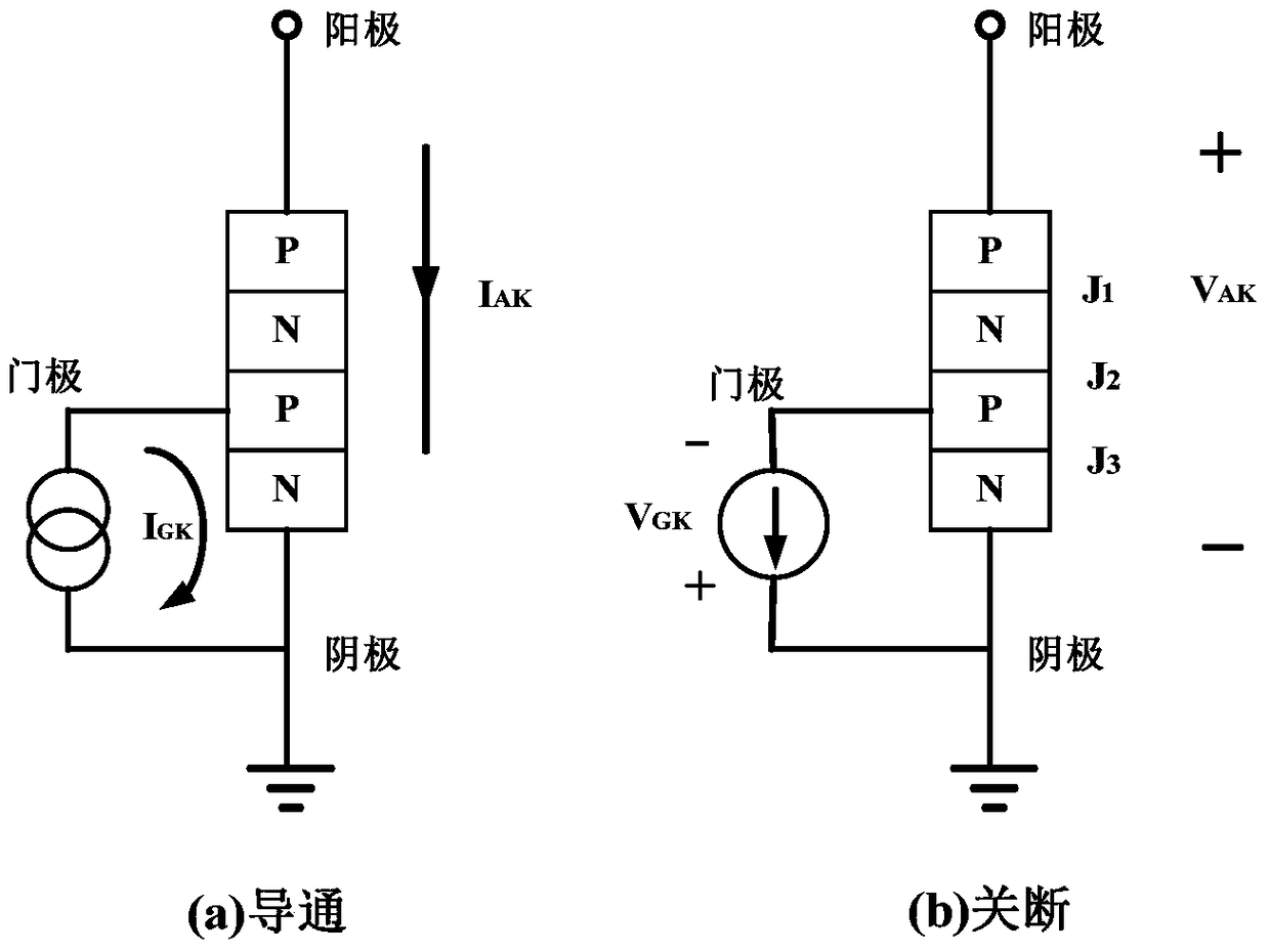
[0062] In order to overcome the deficiency of the GCT chip, it is possible to make the external drive power V GK Larger, and can make the p+ short base region form a current channel with a sufficiently low resistivity. The present invention proposes a GCT with a gate-cathode structure with double p-base regions. The specific implementation structure of the GCT chip is as follows Figure 8 shown. The GCT chip includes more than one cell, and the single cell structure includes from the cathode surface to the anode surface: n+ emitter (cathode), p base region 2, p+ short base region, p base region 1, n-substrate, n' buffer zone, p+ emitter (anode) and cathode surface metal electrode, gate surface metal electrode, anode surface metal electrode.

[0063] In the GCT chip structure proposed by the ...


PUM


Abstract

The invention relates to a gate commutated thyristor having a dual-p-base-region gate cathode structure and a preparation method thereof, and belongs to the technical field of semiconductor integrated circuits. The gate commutated thyristor comprises more than one chip cell. Each chip cell is composed of a p+ emitter electrode, an n' buffer region, an n- buffer region, a p base region 1, a p base region 2, a p+ short base region, an n+ emitter electrode, an anode metal electrode, a gate metal electrode and a cathode metal electrode. The p+ emitter electrode, the n' buffer region, the n- buffer region, the p base region 1, the p base region 2, the p+ short base region and the n+ emitter electrode are arranged in turn. According to the technical scheme of the invention, the gate metal electrode and the cathode metal electrode are ensured to be in the same plane with the surface of a silicon chip based on the conventional trenching process or the channeling abandonment process on the surface of the n+ emitter electrode and the gate electrode. The gate commutated thyristor is provided with an extra layer of p base region, so that the reverse breakdown voltage of a J3 junction is ensured to be larger. Furthermore, the voltage of an external reverse power supply is increased, so that the commutation speed is improved. The turn-off ability of GCT chips is improved.

Description

technical field [0001] The invention belongs to the technical field of semiconductor integrated circuits, and in particular relates to a semiconductor device structure, in particular to a gate structure design of an integrated gate commutation thyristor used in a natural commutation hybrid DC circuit breaker. Background technique [0002] Integrated Gate Commutated Thyristor (IGCT: Integrated Gate Commutated Thyristor) is a new type of power semiconductor device used in large-capacity power electronic devices. It was first developed by Swiss ABB company and successfully put into the market. IGCT integrates GCT (Gate Commutated Thyristor gate commutated thyristor) chip with anti-parallel diode and gate drive MOSFET, and then connects the gate drive with low inductance at the periphery, combining the turn-off capability of the transistor and Thyristors have low conduction loss and other advantages, and are suitable for natural commutation hybrid DC circuit breakers. [0003] ...

Claims


Application Information

Patent Timeline
Patent Type & Authority Patents(China)
IPC IPC(8): H01L29/08H01L29/10H01L29/745H01L21/28H01L21/332
CPCH01L29/0839H01L29/102H01L29/401H01L29/66393H01L29/745
Inventor 吕纲曾嵘余占清刘佳鹏
Owner TSINGHUA UNIV
Why Eureka
Try Eureka