
Method for eliminating electroplating cavity defects on wafer surface

A wafer and void technology, applied in circuits, electrical components, electrical solid devices, etc., can solve problems such as filling difficulties, and achieve the effect of reducing void defects

Inactive Publication Date: 2016-05-04
SHANGHAI HUALI MICROELECTRONICS CORP
View PDF4 Cites 5 Cited by
  • Summary
  • Abstract
  • Description
  • Claims
  • Application Information

AI Technical Summary

Problems solved by technology

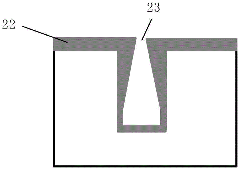
like figure 2 As shown, since the electroplating rate is proportional to the magnitude of the current, using this electroplating method, when the trench 21 of the wafer 20 is filled with electroplating copper, the opening 23 of the trench has a problem of high current density, so that the copper The filling speed of the film 22 at the trench opening 23 is too fast, far exceeding its filling speed at the sidewall and bottom, so that the width of the trench opening is smaller than the width at other positions of the trench sidewall; as image 3 As shown, in this state, when the trench is only partially filled, its opening 23 has become significantly smaller, making filling more difficult; as Figure 4 As shown in , before the copper filling is completed, the opening of the trench has been closed, and finally a void 24 defect is formed under the copper film at the opening

Method used


Image

  • Method for eliminating electroplating cavity defects on wafer surface
  • Method for eliminating electroplating cavity defects on wafer surface
  • Method for eliminating electroplating cavity defects on wafer surface

Examples


Embodiment Construction

[0025] The specific embodiment of the present invention will be further described in detail below in conjunction with the accompanying drawings.

[0026] It should be noted that, in the following specific embodiments, when describing the embodiments of the present invention in detail, in order to clearly show the structure of the present invention for the convenience of description, the structures in the drawings are not drawn according to the general scale, and are drawn Partial magnification, deformation and simplification are included, therefore, it should be avoided to be interpreted as a limitation of the present invention.

[0027] In the following specific embodiments of the present invention, please refer to Figure 5 , Figure 5 It is a flow chart of a method for eliminating the electroplating void defect on the surface of the wafer according to the present invention. Such as Figure 5 Shown, a kind of method of eliminating wafer surface plating cavity defect of th...


PUM


Abstract

The invention discloses a method for eliminating electroplating cavity defects on a wafer surface. Through using a current direction controllable circuit in carrying out electroplating filling to the grooves or through holes of the wafer surface, a current magnitude and direction adjustable circuit is formed; forward and reverse currents are applied to a wafer alternately so as to form an electroplating / etching sequence; in the electroplating process, the wafer surface can be electroplated; the coating film on the wafer surface can be dissociated; therefore, relatively good step coverage rate and good groove (through hole) opening are obtained; the perfect filling process is realized; and the cavity defects formed in the filling process can be reduced.

Description

technical field [0001] The invention relates to the technical field of semiconductor integrated circuit manufacturing, and more specifically, to a method for eliminating electroplating void defects on the surface of a wafer. Background technique [0002] In the manufacturing process of semiconductor integrated circuits, electroplating copper (ECP) is a process of depositing a copper film on the surface of a wafer by electroplating and completing the copper wiring process. It is widely used in the field of advanced semiconductor manufacturing. [0003] see figure 1 , figure 1 It is a schematic diagram of the electroplating principle of the ECP process. Such as figure 1 As shown, in the electroplating tank 10, the wafer 12 to be electroplated is used as the electroplating cathode, the copper material 13 is used as the electroplating anode, and a loop is formed with the power supply, and a forward current is applied to the wafer 12, and the process is carried out in the elec...

Claims


Application Information

Patent Timeline
Patent Type & Authority Applications(China)
IPC IPC(8): H01L21/768C25D3/38C25D5/18C25D7/12
CPCH01L21/76879C25D3/38C25D5/18C25D7/12H01L2221/1068
Inventor 苏亚青文静张传民
Owner SHANGHAI HUALI MICROELECTRONICS CORP
Learn More