
Transmission device and semiconductor processing equipment

A transmission device and preset position technology, which is applied in semiconductor/solid-state device manufacturing, transportation and packaging, conveyor objects, etc., can solve problems such as chip collision or even crushing, unloading chip failure, chip fixation impact, etc., to reduce The probability of chip tilting, avoiding being deflected or crushed, and the effect of avoiding deflection or crushing

Inactive Publication Date: 2016-03-30
BEIJING NAURA MICROELECTRONICS EQUIP CO LTD
View PDF6 Cites 2 Cited by
  • Summary
  • Abstract
  • Description
  • Claims
  • Application Information

AI Technical Summary

Problems solved by technology

However, in practical applications, with the continuous introduction of new processes, more and more types of materials are used in the wafer, such as silicon carbide (SiC), silicon dioxide (SiO2), etc., the adsorption of the electrostatic chuck 11 The capacity requirements are very high, which makes electrostatic adsorption and release difficult. Therefore, in the process of unloading the wafer, it is easy to have the problem of incomplete electrostatic discharge, which is easy to cause the sticking phenomenon, such as Figure 4 As shown, when the ejector pin 12 lifts the wafer at the center of the wafer, part of the edge area of ​​the wafer is still connected to the electrostatic chuck
[0006] Therefore, the following problems often exist in practical applications using the above-mentioned transmission device: since the thimble is arranged in the central area of ​​the electrostatic chuck, the upward force of the thimble is applied to the central area of ​​the wafer, and the sticking generally occurs at the edge area of ​​the wafer. The chip produces a downward force applied to the edge area of ​​the wafer, which will cause the wafer to shift in place when the adhesive chip is released, and the deviation is large, thus causing the wafer to tilt, such as Figure 5 As shown, the edge of the wafer overlaps the edge of the electrostatic chuck, resulting in the failure of unloading the wafer, and even when the robot is transported between the wafer and the electrostatic chuck, the wafer is easily bumped or even broken, resulting in poor transmission stability; , by increasing the requirements for the adsorption capacity of the electrostatic chuck to avoid sticking, but this will affect the fixation of the wafer

Method used


Image

  • Transmission device and semiconductor processing equipment
  • Transmission device and semiconductor processing equipment
  • Transmission device and semiconductor processing equipment

Examples


Embodiment Construction

[0030] In order for those skilled in the art to better understand the technical solution of the present invention, the transmission device and semiconductor processing equipment provided by the present invention will be described in detail below in conjunction with the accompanying drawings.

[0031] Image 6 It is a schematic diagram of the first structure of the transmission device provided by the embodiment of the present invention. Figure 7 for Image 6 Top view of the middle electrostatic chuck. Please also refer to Image 6 with Figure 7, the transport device provided in this embodiment is used to load or unload wafers on the electrostatic tray 22 , which includes a thimble lifting mechanism and a manipulator 20 . Wherein, the thimble lifting mechanism includes a plurality of thimbles 21 and a lifting driver (not shown in the figure), each thimble 21 runs through the upper and lower surfaces of the electrostatic chuck 22, and the lifting driver is used to drive eac...


PUM


Abstract

The invention provides a transmission device and semiconductor processing equipment. The transmission device is used for assembling or disassembling a wafer on a static chuck, and comprises a centre lifting mechanism which comprises a plurality of centres and a lifting driver, wherein each centre passes through the upper and lower surfaces of the static chuck. The lifting driver is used for driving each centre to rise or fall in the static chuck, so as to enable the wafer on the static chuck to be jacked up or enable the wafer on the centres to be placed on the static chuck. The plurality of centres are arranged to be corresponding to the edge region of the static chuck. There are first preset gaps between the plurality of centres and the edge of the static chuck in a radial direction of the static chuck. The transmission device can reduce the probability that the wafer is caused to be inclined because of wafer adhering to great degree, so the transmission device can protect the wafer from being deflected or smashed, can improve the stability and reduces the requirements for the absorption capability of the static chuck.

Description

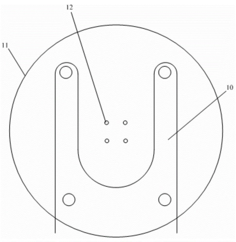
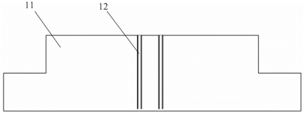
technical field [0001] The invention belongs to the field of semiconductor equipment manufacturing, and in particular relates to a transmission device and semiconductor processing equipment. Background technique [0002] In the technical field of chip manufacturing, inductively coupled plasma (ICP) etching equipment usually uses an electrostatic chuck to fix the wafer and uses a transfer device to load or unload the wafer from the electrostatic chuck. Specifically, before the process, a transfer device is used to load wafers on the electrostatic chuck; during the process, the electrostatic chuck uses electrostatic adsorption to fix the wafer; after the process is completed, the electrostatic chuck performs electrostatic discharge, so that Unload the wafer from the electrostatic chuck. [0003] figure 1 It is a structural schematic diagram of an existing transmission device. figure 2 for figure 1 Cutaway view of the electrostatic chuck in . Please also refer to figure ...

Claims


Application Information

Patent Timeline
Patent Type & Authority Applications(China)
IPC IPC(8): H01L21/677H01L21/67
Inventor 郭宁
Owner BEIJING NAURA MICROELECTRONICS EQUIP CO LTD
Learn More