A kind of wafer tape-out method

A wafer and tape-out technology, applied in the field of wafer tape-out, can solve the problems of fragmentation, high stress of gallium nitride epitaxial layer, wafer warpage, etc.

Active Publication Date: 2018-09-25
FOUNDER MICROELECTRONICS INT
View PDF6 Cites 3 Cited by
  • Summary
  • Abstract
  • Description
  • Claims
  • Application Information

AI Technical Summary

Problems solved by technology

[0003] Since the gallium nitride epitaxial layer grown on the silicon substrate is very stressful, it is very easy to warp the entire wafer, and the existence of stress is also easy to cause the entire wafer to crack and fragment during the subsequent tape-out process. which directly leads to the scrapping of the device

Method used


Image

  • A kind of wafer tape-out method
  • A kind of wafer tape-out method
  • A kind of wafer tape-out method

Examples


Embodiment Construction

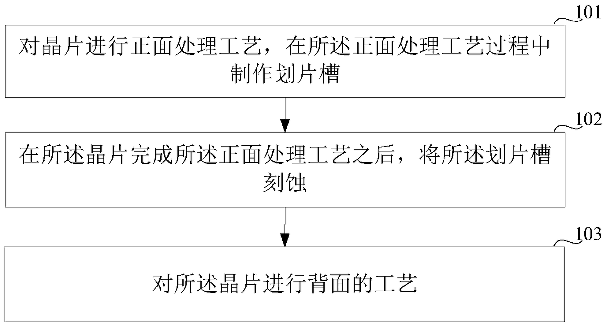
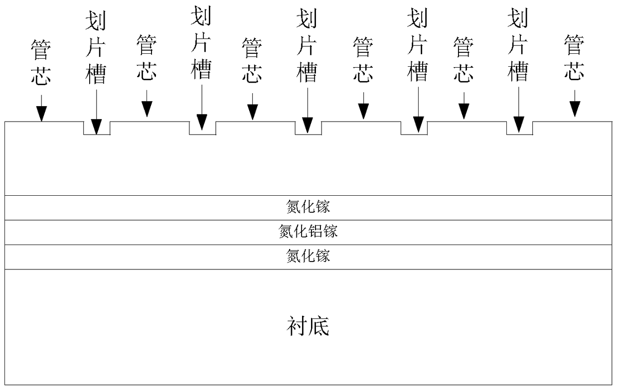
[0025] An embodiment of the present invention provides a wafer tape-out method. In the embodiment of the present invention, the front side treatment process is performed on the wafer, and the scribe groove is made during the front side treatment process; after the front side treatment process is completed on the wafer, the scribe groove is etched; The wafer undergoes backside processing. Since the scribe groove is etched after the front-side treatment process, the stress inside the wafer can be released, which greatly reduces the risk of subsequent steps such as thinning the back gold and other debris fragments.

[0026] In order to make the purpose, technical solutions and beneficial effects of the present invention more clearly understood, the present invention will be further described in detail below in conjunction with the accompanying drawings and embodiments. It should be understood that the specific embodiments described here are only used to explain the present inven...


PUM


Abstract

An embodiment of the invention relates to the technical field of a semiconductor and especially relates to a wafer tapeout method so as to improve stress status of a wafer. The method comprises the following steps: carrying out front-side treatment process on the wafer to prepare scribing grooves in the front-side treatment process; after the front-side treatment process of the wafer, etching the scribing grooves; and carrying out back-side process on the wafer. The scribing grooves are etched after the front-side treatment process, so that the stress inside the wafer can be released, and the risk of wafer fragmenting and breaking in the follow-up process, such as back thinning, is reduced greatly.

Description

technical field [0001] The invention relates to the technical field of semiconductors, in particular to a wafer tape-out method. Background technique [0002] In recent years, the international semiconductor industry has entered the era of the third-generation wide bandgap semiconductor represented by gallium nitride (GaN) and silicon carbide (SiC). [0003] Since the gallium nitride epitaxial layer grown on the silicon substrate is very stressful, it is very easy to warp the entire wafer, and the existence of stress is also easy to cause the entire wafer to crack and fragment during the subsequent tape-out process. And then directly lead to the scrapping of the device. How to reduce the stress of the gallium nitride epitaxial layer has become a key issue in improving the yield of semiconductors. [0004] To sum up, there is an urgent need for a wafer tape-out method to improve the stress condition of GaN wafers. Contents of the invention [0005] An embodiment of the p...

Claims


Application Information

Patent Timeline
Patent Type & Authority Patents(China)
IPC IPC(8): H01L21/02
Inventor 陈建国谢春诚刘蓬
Owner FOUNDER MICROELECTRONICS INT
Why Eureka
Try Eureka