
Static random memory unit having anti-single event effect

An anti-single event effect, memory unit technology, applied in static memory, digital memory information, information storage, etc., can solve the problems of complex manufacturing process and large device area, and achieve extended feedback time, small parasitic capacitance, and low power consumption Effect

Active Publication Date: 2016-02-10
SHANGHAI INST OF MICROSYSTEM & INFORMATION TECH CHINESE ACAD OF SCI
View PDF4 Cites 2 Cited by
  • Summary
  • Abstract
  • Description
  • Claims
  • Application Information

AI Technical Summary

Problems solved by technology

[0009] In view of the above-mentioned shortcomings of the prior art, the object of the present invention is to provide a SRAM unit resistant to single event effects, which is used to solve the complicated manufacturing process caused by the introduction of resistors and capacitors in the random SRAM in the prior art. The problem of large device area

Method used


Image

  • Static random memory unit having anti-single event effect
  • Static random memory unit having anti-single event effect
  • Static random memory unit having anti-single event effect

Examples


Embodiment 1

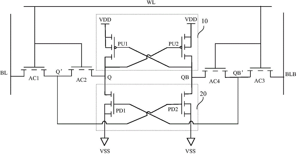
[0040] Such as image 3 As shown, the present invention provides a single-event-resistant SRAM unit, which at least includes: a first cross-coupled inverter 10 , a second cross-coupled inverter 20 and a transmission tube.

[0041] The first cross-coupled inverter 10 is composed of a first pull-up transistor and a second pull-up transistor. As an example, both the first pull-up transistor and the second pull-up transistor are PMOS transistors, which are denoted as PU1 and PU2 respectively. The dimensions of the two pull-up tubes are strictly matched to increase the stability of the storage unit.

[0042] The second cross-coupled inverter 20 is composed of a first pull-down transistor and a second pull-down transistor. As an example, both the first pull-down transistor and the second pull-down transistor are NMOS transistors, which are denoted as PD1 and PD2 respectively. The dimensions of the two pull down tubes are strictly matched to increase the stability of the storage uni...

Embodiment 2

[0053] Such as Figure 4 As shown, the present invention provides another anti-single event effect SRAM unit, the memory unit at least includes: a first cross-coupled inverter 10 , a second cross-coupled inverter 20 and a transmission tube.

[0054] The first cross-coupled inverter 10 is composed of a first pull-up transistor and a second pull-up transistor. As an example, both the first pull-up transistor and the second pull-up transistor are PMOS transistors, which are denoted as PU1 and PU2 respectively. The dimensions of the two pull-up tubes are strictly matched to increase the stability of the storage unit.

[0055] The second cross-coupled inverter 20 is composed of a first pull-down transistor and a second pull-down transistor. As an example, both the first pull-down transistor and the second pull-down transistor are NMOS transistors, which are denoted as PD1 and PD2 respectively. The dimensions of the two pull down tubes are strictly matched to increase the stabili...


PUM


Abstract

The invention provides a static random memory unit having an anti-single event effect. The memory unit at least comprises: a first cross-coupling phase inverter being composed of a first pull-up transistor and a second pull-up transistor; a second cross-coupling phase inverter being composed of a first pull-down transistor and a second pull-down transistor; and a pass transistor which is composed of a first access transistor, a second access transistor, a third access transistor and a fourth access transistor. The static random memory unit can effectively prolong the feedback time required of turning the memory unit, so that the anti-single event upset capability of the memory unit can be improved in the situation that recovery time is not changed. The processes of the static random memory unit are completely compatible with digital logic process. The static random memory unit is less in parasitic capacitance, is low in power consumption, has a natural anti-single event latch-up capability and is free of increase of extra process cost.

Description

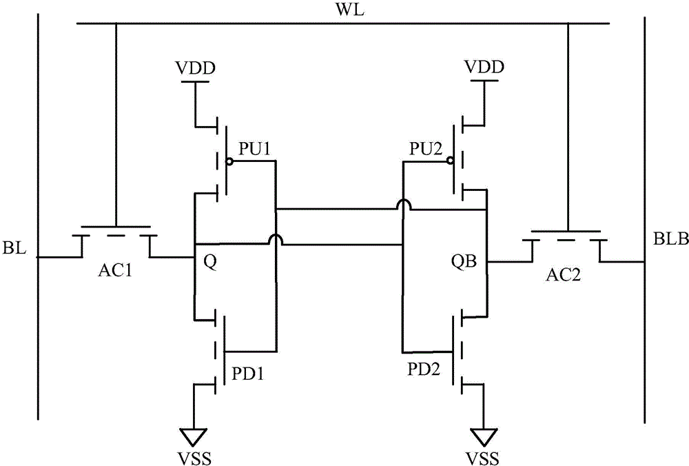
technical field [0001] The invention belongs to the technical field of memory design, and relates to a static random access memory unit, in particular to a static random access memory unit resistant to single event effect. Background technique [0002] Traditional 6T SRAM unit, such as figure 1 As shown, it is composed of two pull-up tubes, pull-down tubes and access tubes; due to the harsh environment in which aerospace electronic equipment works, the memory unit is subject to radiation from various high-energy particles; however, the memory is more sensitive to high-energy particle radiation. Traditional memory cells are generally difficult to meet radiation resistance requirements; therefore, designers often make improvements on the basis of traditional memory cells to improve the radiation resistance of the cells. [0003] Single event effects and total dose effects are the most common and important two types of radiation effects. [0004] The so-called single event ef...

Claims


Application Information

Patent Timeline
IPC IPC(8): G11C11/413
Inventor 陈静何伟伟罗杰馨王曦
Owner SHANGHAI INST OF MICROSYSTEM & INFORMATION TECH CHINESE ACAD OF SCI
Learn More