Heterojunction multiplication layer enhanced algan solar-blind avalanche photodiode and preparation method thereof
An avalanche photoelectric, multiplier layer technology, applied in photovoltaic power generation, circuits, electrical components, etc., can solve the problem of slow development of APD, and achieve the effect of reducing collision ionization, high crystal quality, and reducing device noise
- Summary
- Abstract
- Description
- Claims
- Application Information
AI Technical Summary
Problems solved by technology
Method used
Image
Examples
Embodiment 1
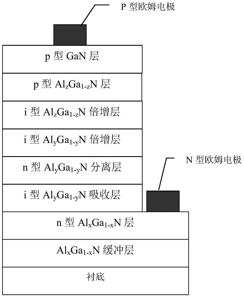
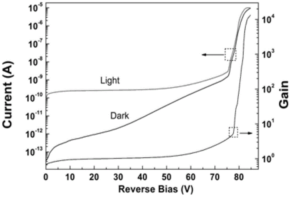
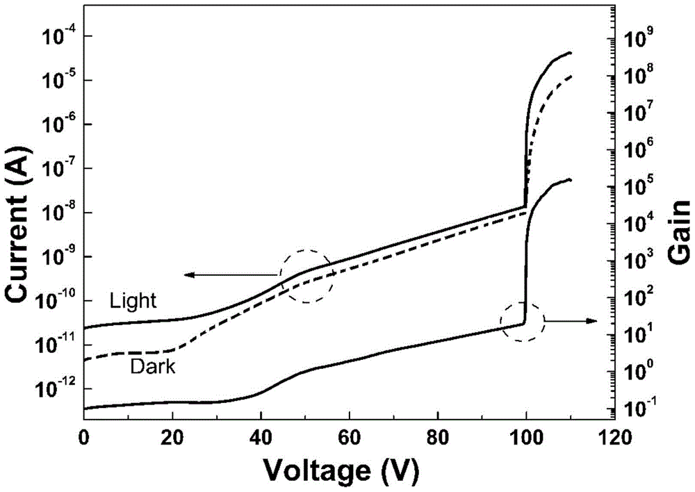
[0042] The steps of this embodiment are basically the same as those of Comparative Example 1, the difference being: (6) in n-type Al 0.4 Ga 0.6 A layer of 120nm i-type Al grown on the N separation layer by MOCVD 0.4 Ga 0.6 N multiplication layer; (7) in i-type Al 0.4 Ga 0.6 A layer of 80nm i-type Al grown on the N multiplication layer by MOCVD 0.2 Ga 0.8 N multiplication layer, in i-type Al 0.2 Ga 0.8 Growth of 87nm p-type Al on the N multiplication layer by MOCVD z Ga 1-z In the N layer, the Al composition z=0.2, using magnesocene as the p-type AlGaN dopant, the doping concentration is 2×10 18 cm -3 . image 3 For the AlGaN ultraviolet avalanche photodetector of this embodiment, the incident light wavelength is 275nm, and the incident light power is 0.01mW / cm 2 Under the test conditions of , the photocurrent, dark current and avalanche multiplication factor obtained under different reverse bias voltages, and figure 2 It can be seen from the comparison that the m...
Embodiment 2
[0044] The steps of this embodiment are basically the same as in Example 1, the difference being that the Al x Ga 1-x The thickness of the N buffer layer is 300nm, the n-type Al x Ga 1-x N layer thickness is 300nm, the i-type Al y Ga 1-y The thickness of the N absorbing layer is 150nm, the n-type Al y Ga 1-y The thickness of the N separation layer is 60nm, the i-type Al y Ga 1-y N multiplication layer thickness is 100nm, the i-type Al z Ga 1-z N multiplication layer thickness is 50nm, the p-type Al z Ga 1-z The thickness of the N layer is 120nm, the thickness of the p-type GaN layer is 30nm, and the composition x=0.8, y=0.6, z=0.3.
Embodiment 3
[0046] The steps of this embodiment are basically the same as in Example 1, the difference being that the Al x Ga 1-x N buffer layer thickness is 600nm, the n-type Al x Ga 1-x N layer thickness is 600nm, the i-type Al y Ga 1-y The thickness of the N absorbing layer is 180nm, the n-type Al y Ga 1-y The thickness of the N separation layer is 80nm, the i-type Al y Ga 1-y N multiplication layer thickness is 150nm, the i-type Al z Ga 1-z N multiplication layer thickness is 100nm, the p-type Al z Ga 1-z The thickness of the N layer is 80nm, the thickness of the p-type GaN layer is 50nm, and the composition x=0.9, y=0.8, z=0.5.
PUM
 Abstract
Description
Claims
Application Information
 - R&D Engineer
- R&D Manager
- IP Professional
- Industry Leading Data Capabilities
- Powerful AI technology
- Patent DNA Extraction
Browse by: Latest US Patents, China's latest patents, Technical Efficacy Thesaurus, Application Domain, Technology Topic, Popular Technical Reports.
© 2024 PatSnap. All rights reserved.Legal|Privacy policy|Modern Slavery Act Transparency Statement|Sitemap|About US| Contact US: help@patsnap.com


