Imaging detector and its manufacturing method

A technology for imaging detectors and manufacturing methods, which is applied in the direction of final product manufacturing, sustainable manufacturing/processing, semiconductor devices, etc., and can solve problems such as poor compatibility, affecting device performance, and complicated processes, so as to save etching steps and ensure quality , Improving the effect of etching technology

Active Publication Date: 2017-03-29
ZHEJIANG JUEXIN MICROELECTRONICS CO LTD
View PDF4 Cites 0 Cited by
  • Summary
  • Abstract
  • Description
  • Claims
  • Application Information

AI Technical Summary

Problems solved by technology

Between the second interconnection hole 30 and the thermistor 20, a metal interconnection line 50 for conductive interconnection is formed. When forming the metal interconnection line 50, a layer of metal interconnection layer is usually formed first, and on the metal interconnection layer A layer of dielectric layer is formed. Due to the existence of the sacrificial layer, dry etching with ashing cannot be used, so wet etching is used to form the metal interconnection line 50, see figure 2 , among the four adjacent interconnection holes v1, v2, v3, and v4 in the second interconnection hole 30 array, the two diagonal interconnection holes v1, v3 and the thermistor 20 are connected to each other, and the other two Two diagonal interconnection holes v3 and v4 are non-conductive interconnection, but the lateral effect of wet etching is serious, which will disconnect the thermistor and the metal layer, resulting in poor connectivity between the upper and lower sides, affecting device performance, and needs to be used The two-step etching process of one-step dry etching of the dielectric layer and one-step wet etching of the metal interconnection layer has poor compatibility and complicated processes

Method used


Image

  • Imaging detector and its manufacturing method
  • Imaging detector and its manufacturing method
  • Imaging detector and its manufacturing method

Examples


Embodiment Construction

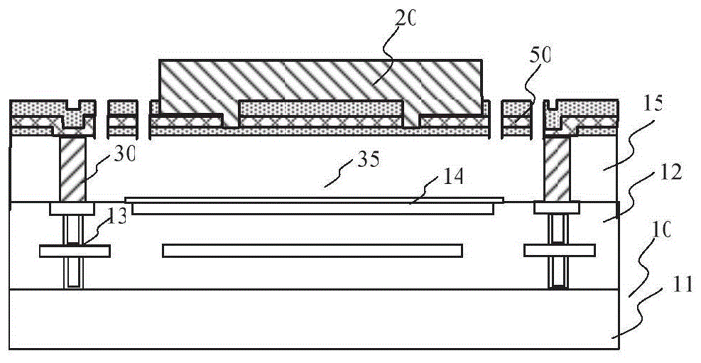
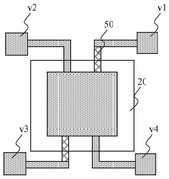
[0029] refer to figure 2 , in the traditional manufacturing method of imaging detectors, taking a detection unit as an example, it includes four interconnection holes v1, v2, v3, v4 arranged on the four corners of a rectangle, and a The thermistor 20, wherein the two diagonal interconnection holes v1, v3 are connected to the thermistor 20 through the metal interconnection line 50, and the other two diagonal interconnection holes v2, v4 are through the metal layer covered with the dielectric layer. The interconnection wire is connected to the thermistor, which plays the role of supporting balance. When the detector is working, the thermistor can convert the optical signal into an electrical signal, so as to output the detected optical signal through an input and an output metal interconnection wire. However, in traditional technology, wet etching is usually used, that is, to cover the position that does not need to be removed with a mask, and then immerse it in the etching so...


PUM

PropertyMeasurementUnit
thicknessaaaaaaaaaa
thicknessaaaaaaaaaa
thicknessaaaaaaaaaa

Abstract

The invention discloses a manufacturing method for an imaging detector, and the method comprises the steps: etching a sacrificial layer on a substrate, and forming a through hole which enables a first interconnection to be exposed; placing a conductive material in the through hole, and forming a second interconnection hole; forming a metal layer; forming a second dielectric layer on the metal layer; removing the second dielectric layer and the metal layer of a partial region through a dry etching method, enabling four adjacent second interconnection holes to be connected to a position above a reflection layer through four metal lines and the second dielectric layers on the four metal lines, and connecting the metal lines of the other two diagonal second interconnection holes covered by the second dielectric layer; Moreover, the dry etching method does not have an ashing step, and a thermistor is formed on the second dielectric layer corresponding to the reflection layer. The thermistor covers the exposed metal lines extending towards a part above the reflection layer. The method modifies the drying etching method, removes the ashing step, and achieves the etching of silicon nitride and the metal layer at the same step through the step of etching a silicon nitride material.

Description

technical field [0001] The invention relates to the field of semiconductor manufacturing, in particular to an imaging detector and a manufacturing method thereof. Background technique [0002] Microelectromechanical systems (MEMS for short) is a multi-disciplinary frontier research field developed on the basis of microelectronics technology. It is a technology that uses semiconductor technology to manufacture microelectromechanical devices. Compared with traditional electromechanical devices, MEMS devices have obvious advantages in high temperature resistance, small size, and low power consumption. After decades of development, it has become one of the world's major scientific and technological fields. It involves electronics, machinery, materials, physics, chemistry, biology, medicine and other disciplines and technologies, and has broad application prospects. [0003] An imaging detector is a transducer that converts an optical signal into an electrical signal. The struc...

Claims


Application Information

Patent Timeline
Patent Type & Authority Patents(China)
IPC IPC(8): H01L31/18H01L31/02
CPCY02P70/50
Inventor 杨天伦毛剑宏
Owner ZHEJIANG JUEXIN MICROELECTRONICS CO LTD
Why Eureka
Try Eureka