A kind of silicon wafer etching method for semiconductor integrated circuit

An integrated circuit and semiconductor technology, which is applied in the field of silicon wafer etching for semiconductor integrated circuits, can solve the problems of insufficient etching, poor etching effect, hindering the contact between the silicon wafer and the etching gas, etc., so as to improve the etching speed and improve the efficiency of etching. Efficiency, easy operation, simple structure effect

Active Publication Date: 2021-03-19
深圳市盛鸿运科技有限公司
View PDF6 Cites 0 Cited by
  • Summary
  • Abstract
  • Description
  • Claims
  • Application Information

AI Technical Summary

Problems solved by technology

During the etching process of silicon wafers, gaseous reaction products will be formed. When the etching temperature does not reach the boiling point of the gaseous products, the gaseous reaction products will remain on the surface of the silicon wafer, hindering the contact between the silicon wafer and the etching gas. , leading to insufficient etching and poor etching effect

Method used


Image

  • A kind of silicon wafer etching method for semiconductor integrated circuit
  • A kind of silicon wafer etching method for semiconductor integrated circuit

Examples


Embodiment Construction

[0026] In order to make the technical means, creative features, goals and effects achieved by the present invention easy to understand, the present invention will be further described below in conjunction with specific embodiments.

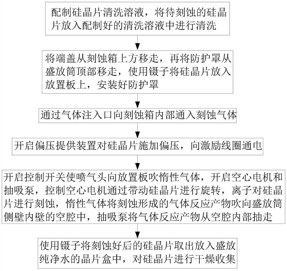
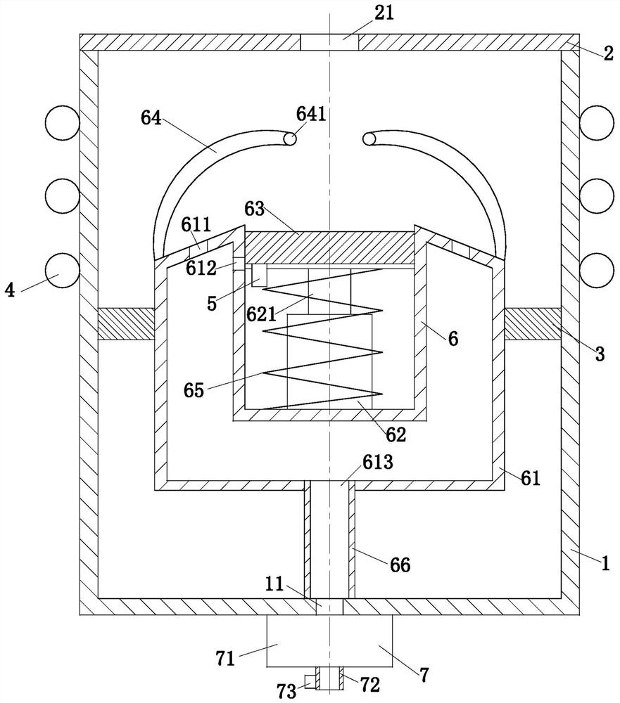
[0027] Such as figure 1 and figure 2 As shown, a silicon wafer etching method for a semiconductor integrated circuit according to the present invention, the etching method adopts the following etching equipment, the etching equipment includes an etching box 1, an end cover 2, a fixing seat 3, an excitation coil 4. Bias voltage supply device 5, holding unit 6 and rotating unit 7. The etching box 1 is a cylinder without a cover, the central axis of the etching box 1 is placed vertically, and a gas outlet is opened in the bottom center of the etching box 1 11 and the No. 1 annular groove, the No. 1 annular groove is located at the outside of the gas outlet 11, and the gas outlet 11 is used for the outflow of gas products etched inside the etching box...


PUM


Abstract

The invention belongs to the technical field of the semiconductor process, and specifically a silicon wafer etching method for a semiconductor integrated circuit. The etching method comprises etchingequipment; the etching equipment comprises an etching tank, an end cover, a fixed seat, an excitation coil, a bias providing device, a placing unit and a rotating unit; the etching tank is a cover-free cylinder, the end cover is placed at the top of the etching tank; the fixed seat is arranged on the inner wall of the etching tank; the excitation coil is used for motivating the etching gas into plasma; the bias providing unit is used for exerting bias on the silicon wafer; the placing unit is used for placing a to-be-etched silicon wafer; the rotating unit is used for driving the placing unitin the etching tank to rotate; the silicon wafer is placed in the placing unit when needing to be etched, the etching gas is imported into the etching tank, so that the silicon wafer is etched under the effect of the excitation coil and the bias providing device. Through the method provided by the invention, the condition that the etching on the silicon wafer is insufficient since the etching product covers the silicon wafer can be timely avoided, and the etching efficiency is improved.

Description

technical field [0001] The invention belongs to the technical field of semiconductor technology, in particular to a silicon wafer etching method for semiconductor integrated circuits. Background technique [0002] Silicon wafers, also known as wafers, are processed from silicon ingots. Millions of transistors can be etched on silicon wafers through special processes, and are widely used in the manufacture of semiconductor integrated circuits. Silicon wafers are the main raw material for the production of semiconductor integrated circuits. Semiconductor silicon wafers are usually drawn from high-purity polycrystalline silicon ingots using the Chaclos method CZ Method to form silicon single crystal ingots with different resistivities, and then go through crystal orientation → cylindrical barrel grinding → processing of the main and auxiliary reference surfaces → slicing → Chamfering→heat treatment→grinding→chemical corrosion→polishing→cleaning→testing→packaging. Among them, ...

Claims


Application Information

Patent Timeline
Patent Type & Authority Patents(China)
IPC IPC(8): H01L21/3065H01L21/67H01J37/32
CPCH01J37/32871H01L21/3065H01L21/67069H01L21/67115
Inventor 徐亚琴李保振
Owner 深圳市盛鸿运科技有限公司
Why Eureka
Try Eureka