On-chip power source noise peak value measurement system suitable for integrated circuit chip and measurement method of measurement system
A technology of power supply noise and integrated circuits, applied in the field of measurement systems for real-time detection of power supply noise peaks on-chip, can solve problems such as slow measurement rate, no power supply noise peaks involved, high power consumption, etc., achieve low measurement accuracy and avoid abnormal power consumption , The effect of low system power consumption
- Summary
- Abstract
- Description
- Claims
- Application Information
AI Technical Summary
Problems solved by technology
Method used
Image
Examples
Embodiment 1
[0184] The test carried out by applying the power supply noise peak measurement module designed by the present invention:
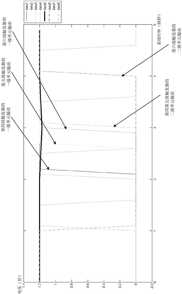
[0185] HSPICE software (version 2008 and above) is used for testing. This test uses the Nangate45nm open source library to add noise to the power supply network. The reference power supply voltage is 1.20V, the noise peak value is 1.17V, and the noise influence time is 1ns. First generate a digital signature lookup table. After that, the power supply plus noise is tested, and the simulation results are as follows: Figure 3D with Figure 3E ( Figure 3E yes Figure 3D As shown in the color display), when the noise comes, the measurement module responds quickly. As the voltage of the power supply network drops, the fourth inverter, the fifth inverter and the sixth inverter successively flip over, making the fourth The output of the first-level trigger units of the group flip-flops, the fifth group of flip-flops, and the sixth group of flip-flops change...
Embodiment 2
[0193] The test carried out by applying the power supply noise peak adjustment module designed by the present invention:
[0194] Use HSPICE software (version 2008 and above) to test, the power supply voltage without noise in this test is 1.20V, and the power supply voltage drops to 1.08V due to noise.
[0195] When there is no noise in the power supply, the output of the delay-sensitive path tested is as follows Figure 4AShown by the black line segment; when the power supply contains noise, apply the same input to the input end of the path, if the adjustment measures of the present invention are not taken, its output is as follows Figure 4B As shown, it is obvious that an error has occurred in its output; the path is adjusted using the present invention, and its output is as follows Figure 4C shown.
[0196] through Figure 4C and Figure 4A In contrast, the high and low level logics of the two are the same at the same sampling time, and the reason why the output wavef...
PUM
 Abstract
Description
Claims
Application Information
 - R&D
- Intellectual Property
- Life Sciences
- Materials
- Tech Scout
- Unparalleled Data Quality
- Higher Quality Content
- 60% Fewer Hallucinations
Browse by: Latest US Patents, China's latest patents, Technical Efficacy Thesaurus, Application Domain, Technology Topic, Popular Technical Reports.
© 2025 PatSnap. All rights reserved.Legal|Privacy policy|Modern Slavery Act Transparency Statement|Sitemap|About US| Contact US: help@patsnap.com


