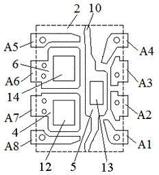
Lead wire framework based on DIP multiple substrates and method of using lead wire framework to manufacture packaging part
A lead frame and package technology, which is applied in the field of lead frames based on DIP multi-base islands, can solve the problems of multiple encapsulation resins, small number of chips, single function, etc., achieve packaging cost savings, increase packaging yield, and reduce consumption Effect
- Summary
- Abstract
- Description
- Claims
- Application Information
AI Technical Summary
Problems solved by technology
Method used
Image
Examples
Embodiment 1
[0080] Using an 8-12 inch wafer thickness thinning machine, the wafer is thinned under the condition of the spindle speed of 2400rpm. The thickness of the chip obtained by thinning is 380μm, and the surface roughness of the chip is Ra0.10mm; the thinning process is the same as that of conventional QFN thinning , coarse grinding + fine grinding and polishing; on the 8-12 inch wafer dicing machine, the chip is diced by using the general dicing process of DIP package; Pick up the first IC chip from the wafer, place it on the adhesive of the first base island, complete the bonding of the first IC chip on the first frame unit, and then bond it on the fourth base island of the second frame unit For the first IC chip, the bonding of the first IC chip on each frame unit of the entire frame is carried out sequentially. After the first IC chip of the entire frame is bonded, the bonding of the first IC chip of the second frame is carried out until the entire frame The first IC chip of th...
Embodiment 2
[0082] Wafer thinning, dicing and core loading are carried out using the method of Example 1. The spindle speed during wafer thinning is 3000rpm, the lifting height of the core on the suction nozzle is 6500step, the lifting height of the thimble is 160mm, and the thimble is rising. The delay time is 10ms, the dispensing height is 2000step, the thickness of the adhesive is 38μm, the pick-up force of the adhesive is 1N, and the adhesive force of the adhesive is 1N; Baking nitrogen flow rate > 0.8m 2 / h; pressure welding according to the method of Example 1: using a suitable copper wire process, the substrate heating temperature is 220 ° C, the ignition flow rate is adjusted to 3100 μA, the ignition discharge time is adjusted to 710 μs, and the copper ball head is melted to obtain a smooth surface And flawless gold ball FAB, the time of 13ms ultrasonic wave and pressure is added to the wiring chopper, the ultrasonic frequency is 130KHZ, the output mode is current, the power is ab...
Embodiment 3
[0084] Wafer thinning, dicing and core loading are carried out using the method of Example 1. The spindle speed during wafer thinning is 2700rpm, the lifting height of the core on the suction nozzle is 5250step, the lifting height of the thimble is 130mm, and the thimble rises The delay time is 7.5ms, the dispensing height is 1700step, the thickness of the adhesive is 23μm, the pick-up force of the adhesive is 0.75N, and the adhesive force of the adhesive is 0.75N; after the core is completed, it is baked for 3 hours using the anti-separation layer baking process , curing and baking nitrogen flow > 0.8m 2 / h; pressure welding is carried out according to the method of Example 1: adopt a suitable copper wire process, the substrate heating temperature is 210°C, adjust the ignition flow rate to 2850μA, adjust the ignition discharge time to 670μs, and melt the gold ball head to obtain a smooth surface And flawless gold ball FAB, the time of 7ms ultrasonic wave and pressure is added...
PUM
 Abstract
Description
Claims
Application Information
 - Generate Ideas
- Intellectual Property
- Life Sciences
- Materials
- Tech Scout
- Unparalleled Data Quality
- Higher Quality Content
- 60% Fewer Hallucinations
Browse by: Latest US Patents, China's latest patents, Technical Efficacy Thesaurus, Application Domain, Technology Topic, Popular Technical Reports.
© 2025 PatSnap. All rights reserved.Legal|Privacy policy|Modern Slavery Act Transparency Statement|Sitemap|About US| Contact US: help@patsnap.com


