Gallium-doped crystalline silicon with uniformly distributed resistivity and preparation method thereof
A technology of resistivity distribution and crystalline silicon, applied in the field of preparation of gallium-doped crystalline silicon, can solve the problems of inability to carry out production and promotion, complex impurity composition, serious silicon wafer compensation, etc.
- Summary
- Abstract
- Description
- Claims
- Application Information
AI Technical Summary
Problems solved by technology
Method used
Image
Examples
preparation example Construction
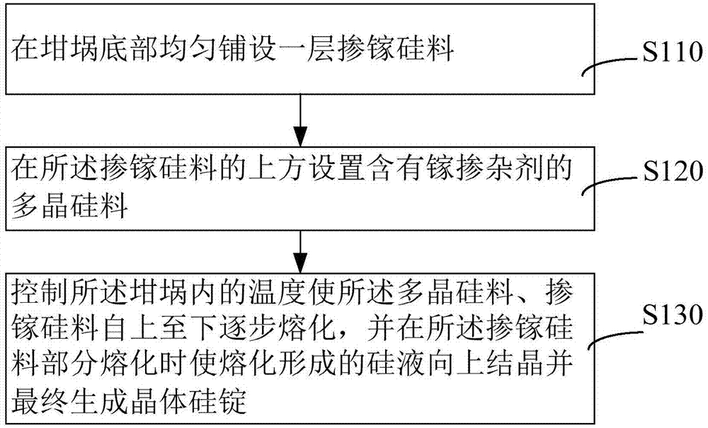
[0020] Please refer to figure 1 , The invention provides a method for preparing gallium-doped crystalline silicon with uniform resistivity distribution, comprising the following steps.
[0021] Step S110, evenly laying a layer of gallium-doped silicon material on the bottom of the crucible. The gallium-doped silicon material can be gallium-doped polycrystalline silicon or gallium-doped monocrystalline silicon, which can be prepared by itself or purchased from the market. This layer of gallium-doped silicon material is also used as a seed crystal for subsequent crystal growth after the silicon material is melted.
[0022] Step S120 , disposing a polysilicon material containing gallium dopant above the gallium-doped silicon material. Continue to put polysilicon material and gallium dopant into the crucible. The gallium dopant can be pure gallium or a silicon-gallium alloy. The mixing degree of the polysilicon material and the gallium dopant is not required, they can be mixed...
Embodiment 1
[0033] Lay 20 kg of granular polysilicon material with a gallium concentration of 200,000 ppbw on the bottom of the crucible. Then put 800kg of primary polysilicon material into the crucible and directly dope 11g of pure gallium at the same time. When melting, a top-down method is adopted, and the measurement is assisted by a quartz rod. When the gallium-doped polysilicon material at the bottom is nearly half melted, crystal growth begins and a crystalline silicon ingot is formed. The electrical resistivity of the crystalline silicon ingot was tested after it came out of the furnace. It was 0.72Ω.cm at a distance of 30mm from the head of the silicon ingot, and 2.21Ω.cm at a distance of 40mm from the tail. The qualified ratio between 0.8 and 3Ω.cm was 68.5%.
Embodiment 2
[0035] Lay 30 kg of granular polysilicon material with a gallium concentration of 12000 ppbw on the bottom of the crucible. Then put 800kg of primary polysilicon material into the crucible, and at the same time directly dope about 10g of pure gallium. When melting, a top-down method is adopted, and the measurement is assisted by a quartz rod. When the gallium-doped polysilicon material at the bottom is nearly half melted, crystal growth begins and a crystalline silicon ingot is formed. The resistivity of the crystalline silicon ingot was tested after it was released from the furnace. It was 0.71Ω.cm at a distance of 30mm from the head of the silicon ingot, and 2.65Ω.cm at a distance of 40mm from the tail. The qualified ratio between 0.8 and 3 was 67.2%.
PUM
 Abstract
Description
Claims
Application Information
 - R&D
- Intellectual Property
- Life Sciences
- Materials
- Tech Scout
- Unparalleled Data Quality
- Higher Quality Content
- 60% Fewer Hallucinations
Browse by: Latest US Patents, China's latest patents, Technical Efficacy Thesaurus, Application Domain, Technology Topic, Popular Technical Reports.
© 2025 PatSnap. All rights reserved.Legal|Privacy policy|Modern Slavery Act Transparency Statement|Sitemap|About US| Contact US: help@patsnap.com

