
Copper-palladium-silver alloy bonding wire and method for preparing same

A palladium-silver alloy and bonding wire technology, which is applied in the field of metal bonding wires for microelectronic packaging, can solve the problems of not being fully suitable for packaging, too long tails of the second solder joint, and increased packaging costs, and achieve superior product performance, Ensure the effect of adhesion and material density

Active Publication Date: 2015-08-12
王东明
View PDF9 Cites 7 Cited by
  • Summary
  • Abstract
  • Description
  • Claims
  • Application Information

AI Technical Summary

Problems solved by technology

Due to the high price of bonding gold wire, the packaging cost increases; the price of pure silver gold-plated bonding wire is relatively low, but in LED, COB and multi-pin integrated circuit packaging technology, inert gas protection is required, but oxidation will still occur , The material is too hard, the ball at the first solder joint, the tail of the second solder joint is too long, etc.
Therefore, bonding gold wire and pure silver gold-plated bonding wire are not completely suitable for packaging of LED, COB and multi-pin integrated circuits

Method used


Image

  • Copper-palladium-silver alloy bonding wire and method for preparing same
  • Copper-palladium-silver alloy bonding wire and method for preparing same
  • Copper-palladium-silver alloy bonding wire and method for preparing same

Examples


Embodiment 1

[0054] 1) Select copper ingots with a purity of ≥99.9999%, palladium ingots with a purity of ≥99.9999%, and silver ingots with a purity of ≥99.9999%, first wash them with 10% sodium hydroxide, then rinse them with deionized water, and dry them in an oven for later use.

[0055]2) Prepare copper-palladium-silver alloy ingots: Put copper ingots with a purity of ≥99.9999%, palladium ingots with a purity of ≥99.9999%, silver ingots with a purity of ≥99.9999%, and calcium and rare earth into a high-purity graphite crucible, and place In the vacuum casting furnace, medium-frequency induction heating is carried out to 1100°C, and vacuum treatment is performed during the heating process. After the material is completely melted, fill it with high-purity nitrogen and keep it warm for 30 minutes. Pour the liquid copper-palladium-silver alloy into a high-purity graphite tank to obtain a copper-palladium-silver alloy ingot with a width of 5 cm, a thickness of 1 cm, and a palladium content ...


PUM

PropertyMeasurementUnit
diameteraaaaaaaaaa
diameteraaaaaaaaaa
diameteraaaaaaaaaa

Abstract

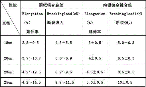
The present invention discloses a copper-palladium-silver alloy bonding wire and a method for preparing the same. The copper-palladium-silver alloy bonding wire is characterized in that a palladium plating protection layer is arranged on the surface of the copper-palladium-silver alloy bonding wire, the diameter of the copper-palladium-silver alloy bonding wire is between 0.015 mm and 0.05 mm, and the thickness of the palladium plating layer is between 0.2 micrometers and 0.6 micrometers. The preparation method comprises the steps of selecting a copper ingot, a palladium ingot and a silver ingot to clean and dry for standby application, preparing a copper-palladium-silver alloy ingot casting, preparing a copper-palladium-silver alloy bar, carrying out homogenizing annealing on the copper-palladium-silver alloy bar, and carrying out the rough tension, the grain refinement annealing, the medium tension, the fine tension, the surface cleaning, the surface palladium plating, the slight tension, the heat treatment, the compound winding and the subpackaging operations orderly. According to the present invention, the copper-palladium-silver alloy bonding wire substitutes for a fine silver gold plating bonding wire, so that the insufficiency of the fine silver gold plating bonding wire is overcome, and the material push-pull effort, the antioxidation performance and the bonding performance of the copper-palladium-silver alloy bonding wire all can reach the performance requirements of the fine silver gold plating bonding wire.

Description

technical field [0001] The invention relates to an alloy bonding wire and a preparation method thereof, in particular to a copper-palladium-silver alloy bonding wire and a preparation method thereof, and belongs to the technical field of metal bonding wires for microelectronic packaging. Background technique [0002] Microelectronic wire bonding is a kind of microelectronic wire bonding that can be tightly welded to the substrate pad by using heat, pressure, and ultrasonic energy to realize the electrical interconnection between the chip and the substrate and the information exchange between the chips. Under ideally controlled conditions, electron sharing or interdiffusion of atoms occurs between the lead and the substrate, enabling atomic-scale bonding between the two metals. [0003] At present, in LED, COB and multi-pin integrated circuit packages, gold wires and pure silver gold-plated wires are mostly used as bonding wires. For example, the applicant's early patent app...

Claims


Application Information

Patent Timeline
Patent Type & Authority Applications(China)
IPC IPC(8): H01L23/49H01L21/48C22C9/00C22C1/02C22F1/08
CPCH01L24/43H01L2224/43H01L2224/45H01L2224/45144H01L2224/45147H01L2224/45565H01L2224/45664H01L2924/00011H01L2924/00012H01L2924/00H01L2924/01206H01L2924/01033H01L2924/01047H01L2924/01046H01L2924/0102
Inventor 王东明李伟文张志富肖冲刘晓丹姜桂萍张莉
Owner 王东明
Learn More