


Quick Research
Generate reliable direction feasibility study reports for your R&D in just a few steps.

Technical Q&A
Discover and master advanced knowledge NOW. Basics, ideas, possibilities, all at once.

Find Solutions
As an expert in R&D theories, this can generate solutions to your technical problems instantly.

Evaluate Feasibility
Analyze your overall solution with one click, know your potential R&D risks in advance.

Monitor Landscape
Get weekly tech updates, stay abreast of the latest tech innovations and key insights.
Epitaxial GaN structure with silylene as buffer layer and preparation method thereof
A technology of buffer layer and silicene layer, which is applied in the field of optoelectronics, can solve the problems of substrate and epitaxial material stress and thermal expansion coefficient mismatch, cracks, and the quality reduction of epitaxial crystals, so as to improve antistatic ability, high crystal quality, and ease Effects of Thermal Expansion Mismatch
- Summary
- Abstract
- Description
- Claims
- Application Information
AI Technical Summary
Problems solved by technology
Method used
Image


Examples
Embodiment 1
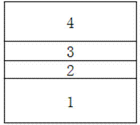
[0030] Such as figure 1 As shown, the epitaxial GaN structure using silicene as a buffer layer in this embodiment includes a silicon carbide substrate 1 , a silicene layer 2 , a silver droplet layer 3 and a GaN layer 4 . The silicene is grown on the silicon carbide substrate 1, a silver droplet layer is deposited on the silicene layer, and the silicene layer and the silver droplet layer on the silicene layer form a buffer layer. Silicon carbide substrate 1 has a thickness of 600 μm. The total thickness of the silicene layer 2 is 0.1 nm, and the number of layers is 1. The thickness of the silver droplet layer 3 is 3000 nm. GaN layer 4 has a thickness of 6 μm.
[0031] The above-mentioned method for preparing the epitaxial GaN structure using silicene as a buffer layer, the steps are as follows:
[0032] (1) The silicon carbide substrate 1 is cleaned, and two layers of silicene layers 2 are prepared on the substrate 1. The total thickness of the silicene layers 2 is 0.1 nm. ...
Embodiment 2
[0037]The silicon substrate 1 in this embodiment has a thickness of 500 μm. The total thickness of the silicene layer is 500 nm, and the number of layers is 300. The thickness of the silver droplet layer 3 is 5 nm. GaN layer 4 has a thickness of 8 μm.
[0038] The above-mentioned method for preparing the epitaxial GaN structure using silicene as a buffer layer, the steps are as follows:
[0039] (1) The silicon carbide substrate 1 is cleaned, and 300 layers of silicene layers 2 are prepared on the substrate 1, and the total thickness of the silicene layers 2 is 500 nm.
[0040] (2) The silver droplet layer 3 is prepared on the silicene layer 2 by metal-organic chemical vapor deposition. Put the substrate 1 prepared with the silicene layer 2 into the MOCVD reaction chamber, heat the temperature to 50° C., and adjust the pressure to 300 mbar to grow silver droplets. The thickness of the silver droplet layer is 5 nm; the carrier gas used is A 1:5 mixture of nitrogen and hydro...
Embodiment 3
[0043] The silicon substrate 1 in this embodiment has a thickness of 100 μm. The total thickness of the silicene layer is 100 nm, and the number of layers is 100. The thickness of the silver droplet layer 3 is 1000 nm. GaN layer 4 has a thickness of 2 μm.
[0044] The above-mentioned method for preparing the epitaxial GaN structure using silicene as a buffer layer, the steps are as follows:
[0045] (1) The silicon carbide substrate 1 is cleaned, and 100 layers of silicene layers 2 are prepared on the substrate 1, and the total thickness of the silicene layers 2 is 100 nm.
[0046] (2) The silver droplet layer 3 is prepared on the silicene layer 2 by metal-organic chemical vapor deposition. Put the substrate 1 prepared with the silicene layer 1 into the MOCVD reaction chamber, heat the temperature to 1000° C., and adjust the pressure to 200 mbar to grow silver droplets. The thickness of the silver droplet layer is 1000 nm; the carrier gas used is A 5:1 mixture of nitrogen ...
PUM
| Property | Measurement | Unit |
|---|---|---|
| Thickness | aaaaa | aaaaa |
| Thickness | aaaaa | aaaaa |
| Thickness | aaaaa | aaaaa |
Abstract
Description
Claims
Application Information
 - R&D Engineer
- R&D Manager
- IP Professional
- Industry Leading Data Capabilities
- Powerful AI technology
- Patent DNA Extraction
Browse by: Latest US Patents, China's latest patents, Technical Efficacy Thesaurus, Application Domain, Technology Topic, Popular Technical Reports.
© 2024 PatSnap. All rights reserved.Legal|Privacy policy|Modern Slavery Act Transparency Statement|Sitemap|About US| Contact US: help@patsnap.com