Vertical structure algan/gan HEMT device and fabrication method thereof

A vertical structure and device technology, applied in the field of microelectronics, can solve problems such as serious current collapse effect, lattice damage, and complexity, and achieve the effects of eliminating the influence of two-dimensional electron gas concentration, enhancing withstand voltage characteristics, and improving withstand voltage characteristics Effect

Active Publication Date: 2018-02-02
SUZHOU NENGWU ELECTRONICS TECH
View PDF5 Cites 0 Cited by
  • Summary
  • Abstract
  • Description
  • Claims
  • Application Information

AI Technical Summary

Problems solved by technology

[0007] However, regardless of the use of Mg ion implantation or doping, on the one hand, lattice damage will be introduced, especially for the current blocking layer, resulting in a large leakage. Diffusion effect, and the leakage and current collapse effects caused by the lattice damage introduced by Al ion implantation are particularly serious. It can only be repaired at a very high temperature, the temperature is about 1350°C, which is more complicated and relatively expensive for industrial use
These defects have always been the bottleneck restricting the current development of vertical structures.

Method used


Image

  • Vertical structure algan/gan HEMT device and fabrication method thereof
  • Vertical structure algan/gan HEMT device and fabrication method thereof
  • Vertical structure algan/gan HEMT device and fabrication method thereof

Examples


Embodiment 1

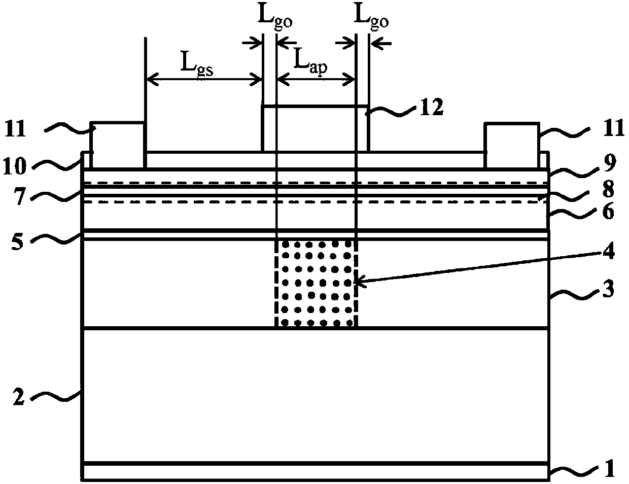
[0053] Example 1 see Figure 4 Shown is a flow chart of a typical manufacturing process of the device of the present invention, but the present invention is not limited to the accompanying drawings and the content described in the following examples, which only use high-resistance GaN as a current blocking layer to achieve conduction and conduction through Si ion implantation. Typical exemplary embodiment of the vertical structure of the hole.

[0054] This embodiment relates to a vertical structure AlGaN / GaN HEMT device using high-resistance GaN as a CBL to form conducting vias through Si ion implantation, which includes the following steps:

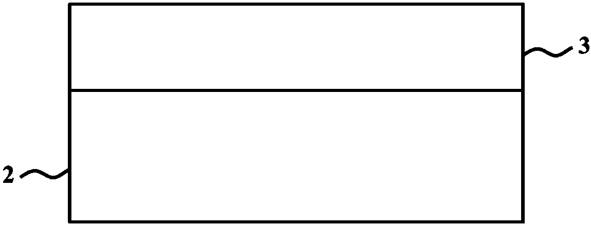
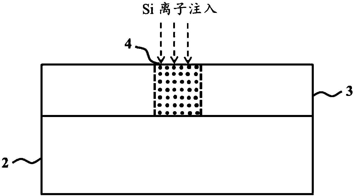
[0055] (1) First, use MOCVD to epitaxially grow a high-resistance GaN layer 2 in the range of hundreds of nanometers to several micrometers. After taking it out of the MOCVD chamber, use an organic solution to clean it and purging it with high-purity nitrogen. See the appendix figure 1 .

[0056] (2) Perform photolithographic developm...


PUM


Abstract

The invention discloses a vertical-structure AlGaN / GaN HEMT device. The device comprises a substrate, an epitaxial structure and source, drain and grid electrodes. The epitaxial structure comprises a current blocking layer, a second semiconductor layer, a first semiconductor layer and a passivation layer which are formed in the front of the substrate successively. Two-dimensional electron gas channels are distributed in the first semiconductor layer and / or the second semiconductor layer. The source electrode is electrically connected with the first semiconductor layer, the grid electrode is arranged on the passivation layer, the drain electrode is arranged on the back of the substrate, a high-resistance GaN layer is used on the current blocking layer, and n-type heavy doped current conduction through holes formed by injection of Si ions are distributed in the area of the high-resistance GaN layer below the grid electrode. The device has the advantages of being high in voltage resistance, low in electric leakage and the like. The invention further discloses a manufacturing method of the HEMT device.

Description

technical field [0001] The invention relates to a semiconductor device, in particular to a vertical structure AlGaN / GaN HEMT epitaxial growth and its manufacturing method, which can be applied to the manufacture of high electron mobility transistors with low on-resistance, high frequency, and high breakdown voltage, belonging to field of microelectronics technology. Background technique [0002] With the rapid development of wireless communication technology, aerospace technology and hybrid vehicles, the development of power devices as the first generation of semiconductor Si and GaAs devices is increasingly unable to meet the problems of high frequency, high power and harsh environments. The more obvious, especially for the relatively low bandgap width and the relatively low critical breakdown voltage of the two, it is difficult to increase in the pursuit of higher power and frequency. The emerging third-generation semiconductor material GaN has wide bandgap, high breakdow...

Claims


Application Information

Patent Timeline
Patent Type & Authority Patents(China)
IPC IPC(8): H01L29/06H01L29/778H01L21/335H01L21/265
CPCH01L21/266H01L29/0688H01L29/778H01L2229/00
Inventor 孙世闯张宝顺范亚明付凯蔡勇于国浩张志利宋亮
Owner SUZHOU NENGWU ELECTRONICS TECH
Why Eureka
Try Eureka