Carbon electrode material of perovskite thin film solar cell and preparation method of carbon electrode material
A technology of solar cells and carbon electrodes, applied in the direction of photosensitive equipment, etc., can solve the problems of large-scale promotion of unsuitable processes, high requirements for experimental conditions, and high energy consumption, and achieve easy control of film thickness, cost reduction, and low energy consumption. Effect
- Summary
- Abstract
- Description
- Claims
- Application Information
AI Technical Summary
Problems solved by technology
Method used
Image
Examples
Embodiment 1
[0023] (1) Preparation of dense titanium dioxide layer
[0024] Put diisopropyl di(acetylacetonate) titanate (TiAcAc) into a beaker, add CH 3 COOH, the molar ratio of raw materials is TiAcAc:CH 3 COOH=1:30, stirred for 0.5 hours, the above solution was sprayed to form a film on the transparent conductive FTO substrate, and the sprayed sample was sintered at 500 ° C for 0.5 hours to prepare a dense titanium dioxide film layer. (2) Preparation and assembly process of solar cells
[0025] Preparation of light-absorbing layer of perovskite film: under inert atmosphere, spin-coat PbI on the above dense titanium dioxide film by liquid phase method 2 solution, heated at 110°C for 5 minutes; impregnated with prepared CH 3 NH 3 I solution, reacted for 30 minutes, took it out and washed it in IPA solution; finally put it in an environment of 70 ° C for 30 minutes to dry.
[0026] (3) Preparation of hole transport layer / carbon electrode layer
[0027] Mix IPA, absolute ethanol, car...
Embodiment 2
[0029] (1) Preparation of dense titanium dioxide layer
[0030] Refer to the preparation process of the dense titanium dioxide layer in Example 1.
[0031] (2) Preparation and assembly process of solar cells
[0032] Refer to the preparation and assembly process of the solar cell in Example 1.
[0033] (3) Preparation of carbon counter electrode:
[0034] Referring to the preparation process of the carbon counter electrode in Example 1, the spraying time was adjusted to 150s.
Embodiment 3
[0036] (1) Preparation of dense titanium dioxide layer
[0037] Refer to the preparation process of the dense titanium dioxide layer in Example 1.
[0038] (2) Preparation and assembly process of solar cells
[0039] Refer to the preparation and assembly process of the solar cell in Example 1.
[0040] (3) Preparation of hole transport layer / carbon electrode
[0041] Referring to the preparation process of the carbon counter electrode in Example 1, the spraying time was adjusted to 50s.
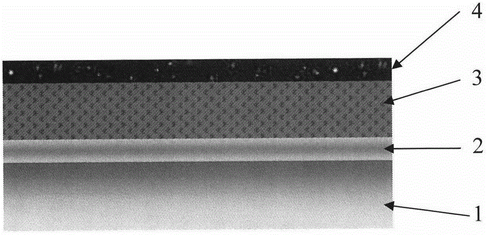
[0042] combined with figure 1 Schematic representation of the structure of a perovskite thin film solar cell, where the hole transport layer / carbon electrode layer is figure 1Schematic diagram of the thin film referred to in middle 4, that is, the carbon electrode layer of the perovskite thin film solar cell.
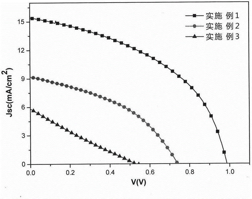
[0043] combine figure 2 and image 3 It can be further illustrated that the operation of the present invention is highly controllable. The resistance of the hole transport lay...
PUM
| Property | Measurement | Unit |
|---|---|---|
| Thickness | aaaaa | aaaaa |
Abstract
Description
Claims
Application Information
 - R&D
- Intellectual Property
- Life Sciences
- Materials
- Tech Scout
- Unparalleled Data Quality
- Higher Quality Content
- 60% Fewer Hallucinations
Browse by: Latest US Patents, China's latest patents, Technical Efficacy Thesaurus, Application Domain, Technology Topic, Popular Technical Reports.
© 2025 PatSnap. All rights reserved.Legal|Privacy policy|Modern Slavery Act Transparency Statement|Sitemap|About US| Contact US: help@patsnap.com


