A method of forming a semiconductor device

A semiconductor and device technology, applied in the field of fully isolated back-illuminated image sensor and its manufacturing, can solve the problem of high cost, achieve the effect of reducing on-resistance, improving production efficiency, and maintaining stable on-resistance

Active Publication Date: 2017-10-20
SHANGHAI HUAHONG GRACE SEMICON MFG CORP
View PDF5 Cites 0 Cited by
  • Summary
  • Abstract
  • Description
  • Claims
  • Application Information

AI Technical Summary

Problems solved by technology

Higher cost due to thick epitaxial growth, deep trench etching, trench filling, etc. involved

Method used


Image

  • A method of forming a semiconductor device
  • A method of forming a semiconductor device
  • A method of forming a semiconductor device

Examples


Embodiment

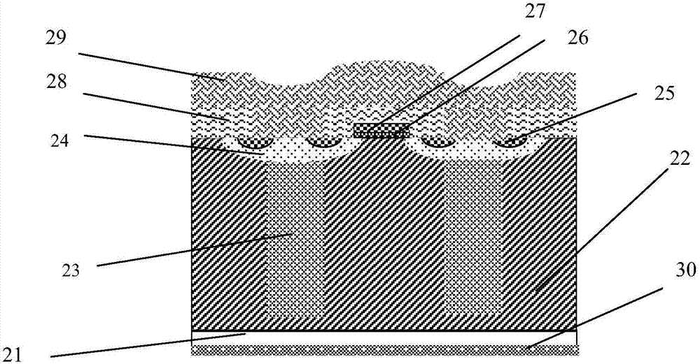
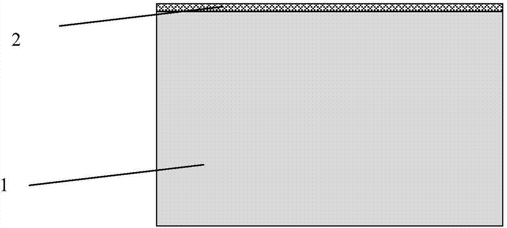
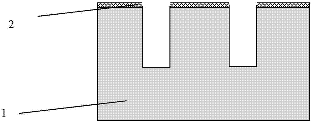
[0033] Such as Figure 2-Figure 12 As shown, a method for forming a semiconductor device of the present invention specifically includes the following steps:

[0034] 1) Grow dielectric layer 2 on semiconductor silicon substrate 1, semiconductor silicon substrate 1 can be N-type or P-type, doping concentration is 1E13-1E17cm -3 ; The dielectric layer 2 is at least one of silicon oxide, silicon nitride, and silicon oxynitride, with a thickness of 0.1 μm-2 μm (see figure 2 ).

[0035] 2) Etching deep trenches on the semiconductor silicon substrate 1, the deep trenches have a width of 1-10 μm, a depth of 10-80 μm, and a trench spacing of 2-15 μm (see image 3 ); and the pre-measured doping concentration of the semiconductor silicon substrate 1 makes the depth of the deep trench positively correspond to the doping concentration of the semiconductor silicon substrate 1, that is, the breakdown voltage of the device is preset, when the semiconductor silicon substrate When the dopi...


PUM

PropertyMeasurementUnit
thicknessaaaaaaaaaa

Abstract

The invention discloses a forming method of a semiconductor device. The method comprises the following steps of 1) etching a deep groove in one side of a semiconductor silicon substrate; 2) performing injection and drive-in on the bottom of the groove; 3) filling the inner part of the groove with a silicon epitaxial layer and leveling the silicon epitaxial layer; and forming a base region, a source region, a grid, a dielectric layer and a front metal electrode; 4) thinning the other side of the semiconductor silicon substrate, and performing ion injection, laser annealing and back metal electrode formation on the other side. By the forming method disclosed by the invention, the breakdown voltage and the on-resistance of the semiconductor device are stabilized through adjusting the silicon epitaxial doping concentration, the groove depth and wafer thickness. By the method disclosed by the invention, the manufacturing cost of superjunction devices can be reduced, the production efficiency can be improved, and the on-resistance of the devices can be reduced.

Description

technical field [0001] The invention belongs to the field of semiconductor integrated circuit manufacturing, in particular to a semiconductor image sensor, in particular to a fully isolated back-illuminated image sensor and a manufacturing method thereof. Background technique [0002] VDMOSFET (VerticalDouble-diffused MOSFET, vertical double-diffused MOS transistor) can reduce the on-resistance by reducing the thickness of the drain drift region. However, reducing the thickness of the drain drift region will reduce the breakdown voltage of the device, so in In VDMOS, increasing the breakdown voltage of the device and reducing the on-resistance of the device are a pair of contradictions. The super-junction MOSFET adopts a new voltage-resistant layer structure - using a series of alternately arranged P-type and N-type semiconductor thin layers to deplete the P-type and N-type regions under the reverse voltage at a lower voltage to achieve mutual charge compensation. As a resu...

Claims


Application Information

Patent Timeline
Patent Type & Authority Patents(China)
IPC IPC(8): H01L21/336H01L21/265
CPCH01L21/26506H01L29/66712
Inventor 刘继全
Owner SHANGHAI HUAHONG GRACE SEMICON MFG CORP
Why Eureka
Try Eureka