Preparation method of porous-silicon-based and multi-dimensional tungsten-oxide composite structure
A porous silicon-based, composite structure technology, applied in the direction of measuring devices, instruments, scientific instruments, etc., can solve the problem of high working temperature of tungsten oxide, achieve the effect of improving sensitivity and selectivity, less process conditions, and simple operation
- Summary
- Abstract
- Description
- Claims
- Application Information
AI Technical Summary
Problems solved by technology
Method used
Image
Examples
Embodiment 1
[0042] (1) Cleaning of silicon substrate
[0043] Cut a 2-inch P-type single-crystal silicon substrate with a resistivity of 10-15Ω·cm, a thickness of 400μm, and a crystal orientation of (100) into a rectangular silicon substrate with a size of 2.4cm×0.9cm. Soak silicon wafers in a mixture of concentrated sulfuric acid and hydrogen peroxide with a volume ratio of 3:1 for 40 minutes, then soak them in a mixture of hydrofluoric acid and deionized water with a volume ratio of 1:1 for 30 minutes, and then soak them in acetone Ultrasonic cleaning with ethanol for 5 minutes, and finally put the silicon substrate into absolute ethanol for later use.
[0044] (2) Preparation of porous silicon
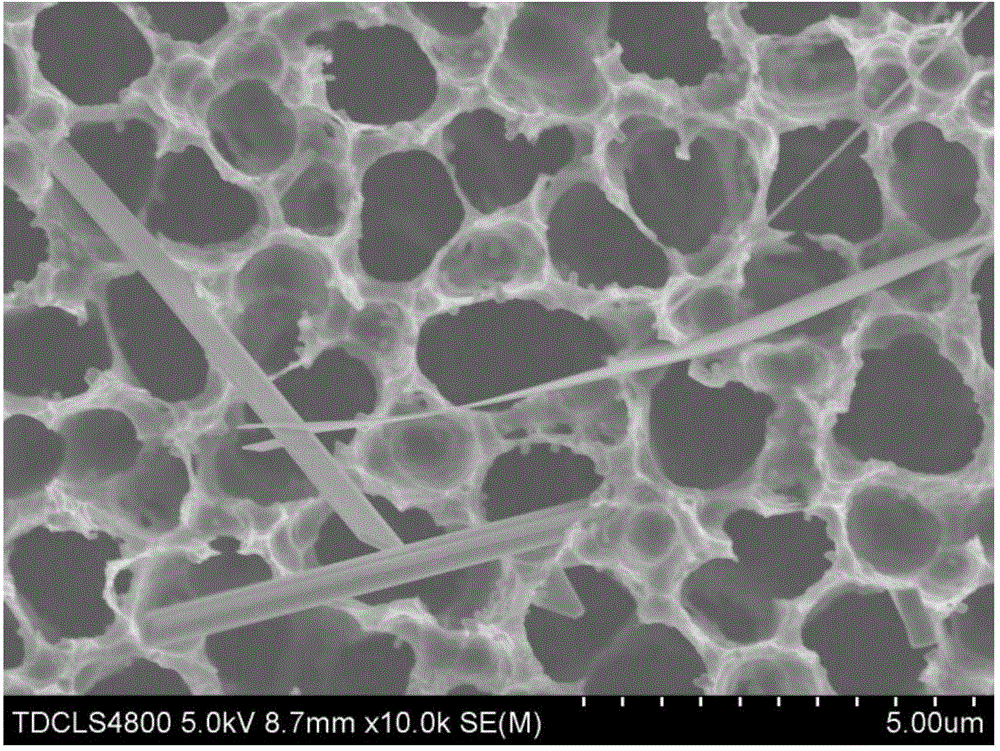
[0045] The porous silicon layer is prepared on the polished surface of the monocrystalline silicon wafer in step (1) by means of double-groove electrochemical etching, and the electrolytic solution used is composed of 40% hydrofluoric acid and 40% dimethylformamide with a mass concentration. ...
Embodiment 2
[0056] The difference between this example and Example 1 is that the heat treatment temperature of the seed layer in step (4) is 550°C, and the scanning electron microscope analysis results of the surface morphology are as follows: Image 6 with Figure 7 As shown, the prepared tungsten oxide is a hierarchical nanostructure of nanoblocks-nanorods.
Embodiment 3
[0058] The difference between this example and Example 1 is that the heat treatment temperature of the seed layer in step (4) is 600°C, and the scanning electron microscope analysis results of the surface morphology are as follows: Figure 8 with Figure 9 As shown, the scanning electron microscope analysis results of the cross-sectional morphology are as follows Figure 10 As shown, the as-prepared one-dimensional tungsten oxide nanorods grow almost parallel to the porous silicon substrate.
PUM
| Property | Measurement | Unit |
|---|---|---|
| Concentration | aaaaa | aaaaa |
| Resistivity | aaaaa | aaaaa |
| Thickness | aaaaa | aaaaa |
Abstract
Description
Claims
Application Information
 - R&D
- Intellectual Property
- Life Sciences
- Materials
- Tech Scout
- Unparalleled Data Quality
- Higher Quality Content
- 60% Fewer Hallucinations
Browse by: Latest US Patents, China's latest patents, Technical Efficacy Thesaurus, Application Domain, Technology Topic, Popular Technical Reports.
© 2025 PatSnap. All rights reserved.Legal|Privacy policy|Modern Slavery Act Transparency Statement|Sitemap|About US| Contact US: help@patsnap.com


