Device and method for monitoring intermetallic dielectric layer

An intermetallic dielectric layer, metal technology, applied in the direction of semiconductor/solid-state device testing/measurement, etc., can solve the problem of inability to judge whether there is abnormality or defect in the intermetallic dielectric layer

Inactive Publication Date: 2015-05-13
PEKING UNIV FOUNDER GRP CO LTD +1
View PDF8 Cites 4 Cited by
  • Summary
  • Abstract
  • Description
  • Claims
  • Application Information

AI Technical Summary

Problems solved by technology

[0006] In view of the above-mentioned defects, the technical problem to be solved in the present invention is how to monitor the state of the intermetallic dielectric layer between the layers of the multilayer metal interconnection, so that it is impossible to judge the intermetallic layer between the multilayer metal interconnection. Whether there is any abnormality or defect in the dielectric layer

Method used


Image

  • Device and method for monitoring intermetallic dielectric layer
  • Device and method for monitoring intermetallic dielectric layer
  • Device and method for monitoring intermetallic dielectric layer

Examples


Embodiment 1

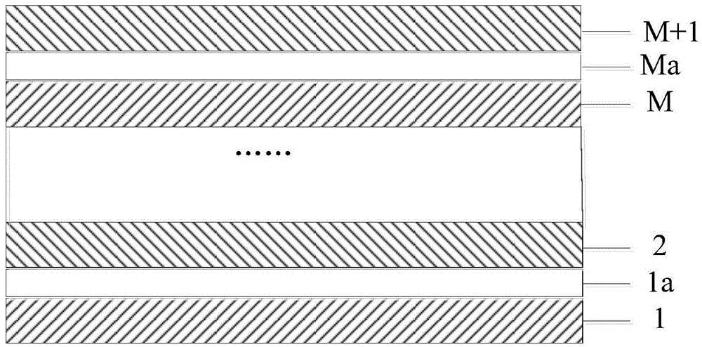
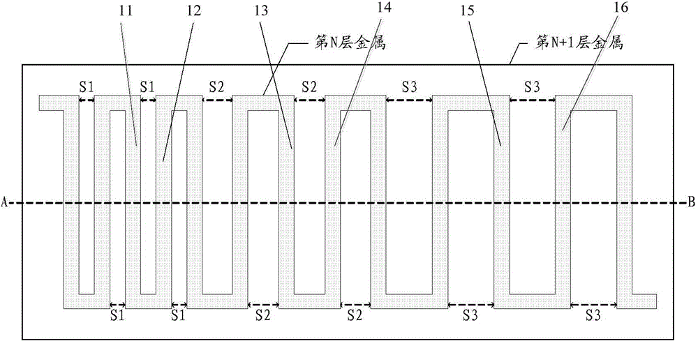
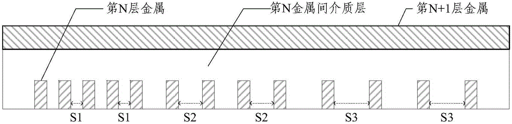
[0028] Embodiment 1 of the present invention provides a device for monitoring an intermetallic dielectric layer, which specifically includes: at least two layers of metals form a stacked structure, wherein the first layer of metals has a wave structure;

[0029] The second layer of metal overlies the first layer of metal.

[0030] By setting the first layer of metal into a corrugated structure, the length and structural complexity of this layer of metal can be increased, and the first layer of metal is completely covered with a large piece of metal, that is, the second layer of metal above the first layer of metal. The contact area between the metal layer and the intermetallic dielectric layer can be increased, which is beneficial to the detection of the leakage phenomenon. The above structural device can effectively monitor defects such as pinholes, poor planarization process and particles in the intermetallic dielectric layer.

[0031] The waveform structure in the above-men...

Embodiment 2

[0042] Based on the above device, the second embodiment of the present invention also provides a method for monitoring the intermetallic dielectric layer using the device for monitoring the intermetallic dielectric layer in the first embodiment above. The method includes: measuring the intermetallic dielectric layer between two layers of metal When the breakdown voltage exceeds the threshold range, it is determined that there is an abnormality in the intermetallic dielectric layer between the two metal layers.

[0043] The above method compares the breakdown voltage of the intermetallic dielectric layer between the two metal layers with a preset threshold range, and if the breakdown voltage exceeds the threshold value range, it is determined that there is an abnormality in the intermetallic dielectric layer between the two metal layers, otherwise the It shows that the intermetallic dielectric layer between two layers of metal is reliable.

[0044] Further, measuring the breakd...


PUM


Abstract

The invention provides a device for monitoring an intermetallic dielectric layer. The device comprises a stacking structure composed of at least two layers of metal, wherein the first layer of metal is of a waveform structure, and the second layer of metal covers the first layer of metal. Because the first layer of metal is of a waveform structure, the length and structure complexity of the layer of metal can be increased. A hunk of metal, namely, the second layer of metal is arranged on the first layer of metal to completely cover the first layer of metal, which can increase the area of contact between the metal layers and an intermetallic dielectric layer, and is conductive to detection of leakage. By adopting the device of the invention, the defects of the intermetallic dielectric layer, such as pinhole, poor flattening workmanship and particles, can be effectively monitored.

Description

technical field [0001] The invention relates to the technical field of semiconductor manufacturing, in particular to a device and method for monitoring an intermetal dielectric layer. Background technique [0002] With the gradual reduction of the processing size of integrated circuits, one layer of metal can no longer complete the wiring work of the entire circuit, so a multi-layer metal interconnection (such as 2-layer, 3-layer or even more-layer metal interconnection) structure must be used. To meet the wiring requirements of the circuit, these multilayer metal interconnections need to be separated by dielectric materials with good insulation properties, and these dielectric materials are intermetallic dielectric layers. Multi-layer metal interconnection lines and inter-metal dielectric layers form a stacked structure. When multiple layers of metal are included, they are named as the first layer of metal, second layer of metal, third layer of metal..., and each layer of i...

Claims


Application Information

Patent Timeline
Patent Type & Authority Applications(China)
IPC IPC(8): H01L21/66
Inventor 潘光燃王焜文燕石金成由云鹏高振杰
Owner PEKING UNIV FOUNDER GRP CO LTD
Why Eureka
Try Eureka