pn junction and its preparation method
A pn junction and n-type technology, which is applied in semiconductor/solid-state device manufacturing, electrical components, circuits, etc., can solve problems such as restricting the application of SnO and limited types of pn junctions, and achieve the goals of reducing edge discharge effects, low cost, and improving performance Effect
- Summary
- Abstract
- Description
- Claims
- Application Information
AI Technical Summary
Problems solved by technology
Method used
Image

Examples
preparation example Construction
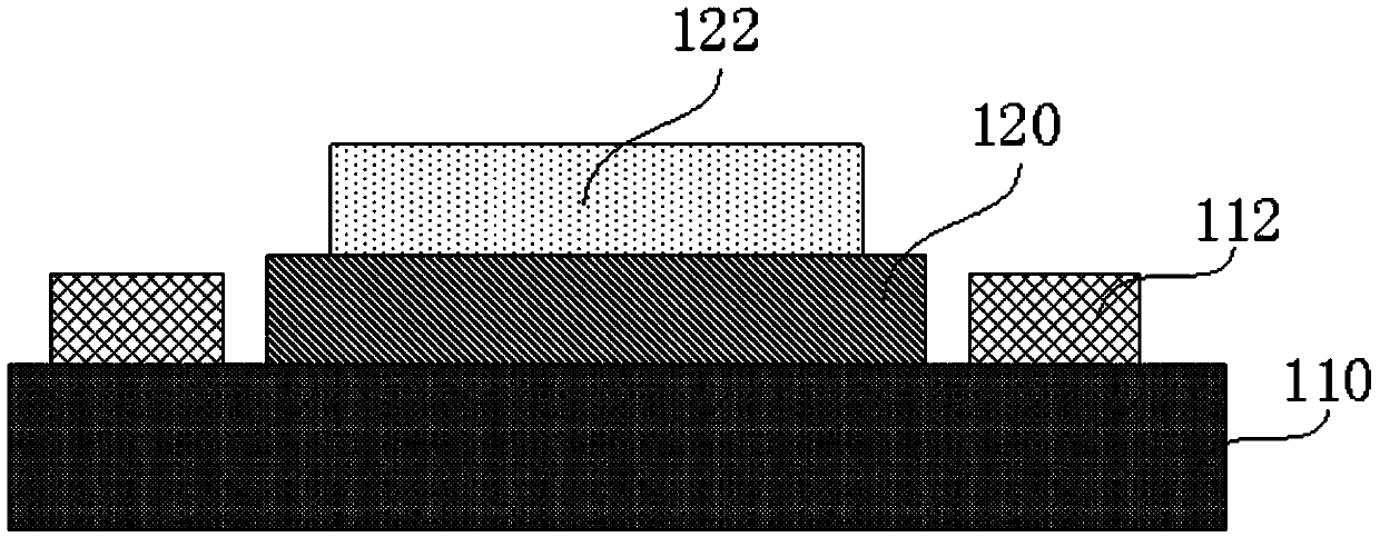
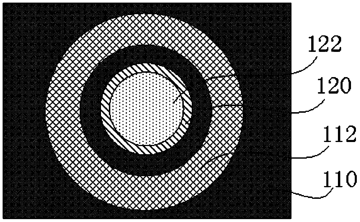
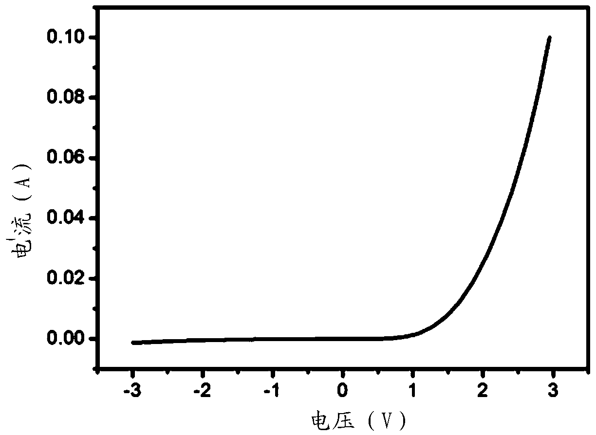
[0054] In the preparation process of the pn junction of the present invention, if the deposition thickness of the p-type SnO semiconductor layer 120 is too small, the performance of the formed pn junction is poor and cannot meet the practical application; if the deposition thickness is too large, not only the cost is increased, Moreover, it is not conducive to the development trend of miniaturization of devices. Therefore, the thickness of the p-type SnO semiconductor layer 120 is preferably 50nm-80nm, within this thickness range, the obtained pn junction has obvious rectifying effect.
[0055] In the pn junction of the present invention, if the cross-sectional area of the electrode is too small, large resistance will be generated, and the preparation is difficult; if the cross-sectional area of the electrode is too large, electric leakage will easily occur and the safety performance of the device will be reduced. Preferably, as an implementation manner, the ratio of the c...
Embodiment 1
[0093] (1) Cut the n-type single-polished silicon wafer with ρ2 Sample silicon wafers, washed and dried;
[0094] (2) Spin-coat a layer of photoresist on the crystal plane of the sample silicon wafer to form a first mask;
[0095] (3) Form a circular window with a diameter of 160 μm by using the first mask of ultraviolet lithography;
[0096] (4) Utilize electron beam evaporation equipment to evaporate the tin dioxide evaporation material at room temperature, and deposit an amorphous SnO semiconductor layer on the circular window to obtain a Si-SnO composite body; wherein, the deposition thickness of the SnO semiconductor layer is 80nm;
[0097] (5) utilizing acetone and deionized water to clean the Si-SnO complex obtained in step (4);
[0098] (6) Place the cleaned Si-SnO composite in a rapid annealing furnace, and anneal at 350° C. for 10 minutes under an argon atmosphere;
[0099] (7) Spin-coat a layer of photoresist on the surface of the Si-SnO composite body after anneal...
Embodiment 2
[0104] (1) Cut the n-type single-polished silicon wafer with ρ2 Sample silicon wafers, washed and dried;
[0105] (2) Spin-coat a layer of photoresist on the crystal plane of the sample silicon wafer to form a first mask;
[0106] (3) Form a circular window with a diameter of 160 μm by using the first mask of ultraviolet lithography;
[0107] (4) Utilize electron beam evaporation equipment to evaporate the tin dioxide evaporation material at room temperature, and deposit an amorphous SnO semiconductor layer on the circular window to obtain a Si-SnO composite body; wherein, the deposition thickness of the SnO semiconductor layer is 80nm;
[0108] (5) utilizing acetone and deionized water to clean the Si-SnO complex obtained in step (4);
[0109] (6) Place the cleaned Si-SnO composite in a rapid annealing furnace, and anneal at 400°C for 10 minutes under an argon atmosphere;
[0110] (7) Spin-coat a layer of photoresist on the surface of the Si-SnO composite body after anneal...
PUM
 Abstract
Description
Claims
Application Information
 - Generate Ideas
- Intellectual Property
- Life Sciences
- Materials
- Tech Scout
- Unparalleled Data Quality
- Higher Quality Content
- 60% Fewer Hallucinations
Browse by: Latest US Patents, China's latest patents, Technical Efficacy Thesaurus, Application Domain, Technology Topic, Popular Technical Reports.
© 2025 PatSnap. All rights reserved.Legal|Privacy policy|Modern Slavery Act Transparency Statement|Sitemap|About US| Contact US: help@patsnap.com