rfldmos device and its manufacturing method

A device and conductivity type technology, applied in the field of semiconductor integrated circuit manufacturing, can solve problems such as insufficient breakdown voltage, reduced device reliability, large leakage current, etc. The effect of reducing process costs

Active Publication Date: 2017-06-06
SHANGHAI HUAHONG GRACE SEMICON MFG CORP
View PDF5 Cites 0 Cited by
  • Summary
  • Abstract
  • Description
  • Claims
  • Application Information

AI Technical Summary

Problems solved by technology

Since the source / drain metal silicide, that is, the metal silicide 111 on the source region 107 and the drain region 108, is deposited in the same step as the gate metal silicide, the thickness of the source / drain metal silicide is too thick, and a large amount of The N-type heavy doping of the source region 107 and the drain region 108 is consumed, resulting in a large leakage current during the reverse breakdown of the RF LDMOS, and the breakdown voltage is not stable enough, resulting in a decrease in device reliability

Method used


Image

  • rfldmos device and its manufacturing method
  • rfldmos device and its manufacturing method
  • rfldmos device and its manufacturing method

Examples


Embodiment Construction

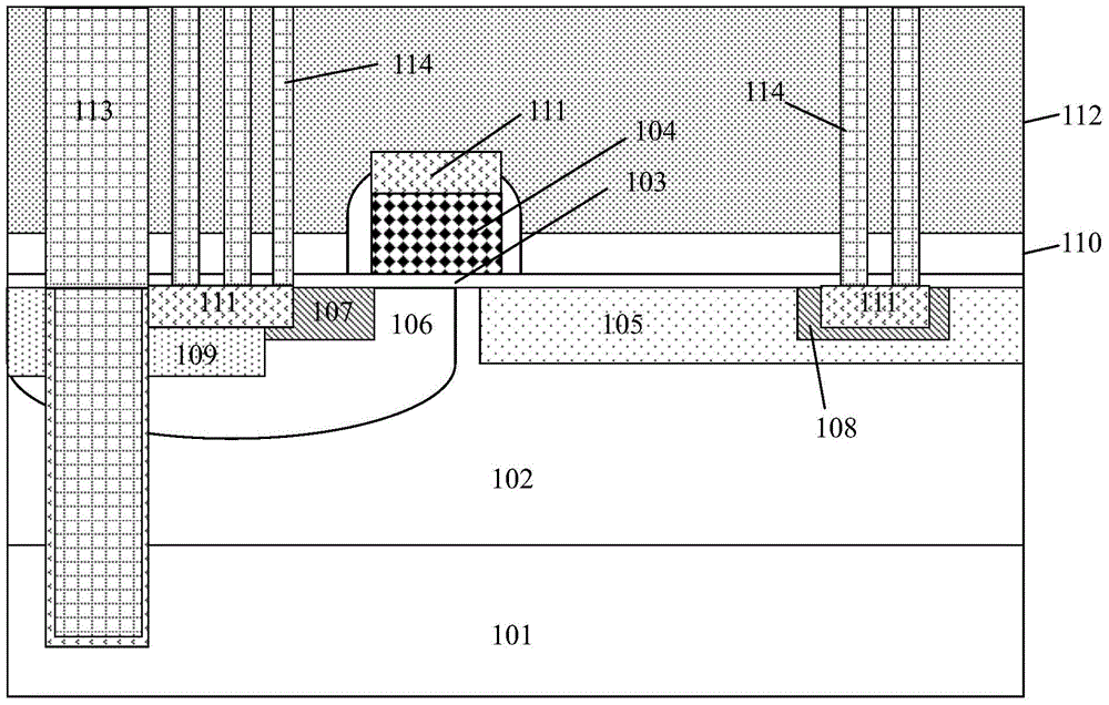
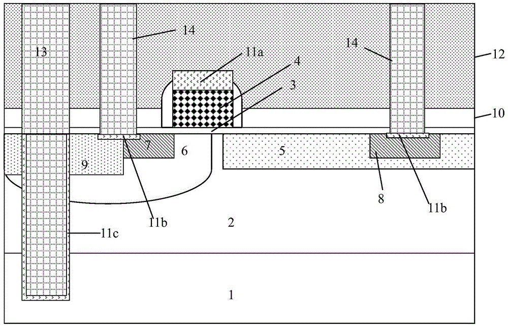
[0051] Such as figure 2 Shown is a schematic structural diagram of the RFLDMOS device of the embodiment of the present invention; the RFLDMOS device of the embodiment of the present invention includes:

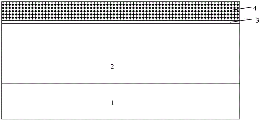
[0052] A heavily doped silicon substrate 1 of the first conductivity type.

[0053] A silicon epitaxial layer 2 doped with the first conductivity type, the silicon epitaxial layer 2 is formed on the surface of the silicon substrate 1 .

[0054] A heavily doped silicon substrate 1 of the first conductivity type. The doping concentration of the silicon substrate 1 is greater than 1e20cm -3 .

[0055] A silicon epitaxial layer 2 doped with the first conductivity type, the silicon epitaxial layer 2 is formed on the surface of the silicon substrate 1 . The doping concentration and thickness of the silicon epitaxial layer 2 depend on the drain terminal operating voltage of the device, the higher the drain terminal operating voltage, the lower the doping of the silicon epitaxial...


PUM

PropertyMeasurementUnit
thicknessaaaaaaaaaa
thicknessaaaaaaaaaa
thicknessaaaaaaaaaa

Abstract

The invention discloses an RFLDMOS device. The thickness of a first metal silicide layer formed on the top surface of a polysilicon gate is greater than that of second metal silicide layers formed on the surfaces of source and drain regions, and the second metal silicide layers are formed on the bottoms of contact holes of the source region and the drain region. The invention further discloses a manufacturing method of the RFLDMOS device. By thickening the first metal silicide layer, the resistance of the gate can be reduced, and low resistance of the gate is easily ensured. By reducing the thickness of the second metal silicide layers, consumption of the second metal silicide layers to second conductivity type heavily doped regions of the source region and the drain region can be reduced, the reverse breakdown voltage of the RFLDMOS device can be stabilized, the breakdown voltage of the device can be integrally increased, and the reliability of the device can be improved. No additional photomask needs to be adopted to define the forming regions of the second metal silicide layers, the steps of the photo-etching process are reduced by one, and the process cost is reduced.

Description

technical field [0001] The invention relates to the field of semiconductor integrated circuit manufacturing, in particular to a radio frequency lateral field effect transistor (RF LDMOS) device; the invention also relates to a method for manufacturing the RF LDMOS device. Background technique [0002] RF Lateral Field Effect Transistor (RF LDMOS) is a common device used in RF base stations and broadcasting stations. Such as figure 1 Shown is a schematic structural diagram of an existing RFLDMOS device. Taking an N-type device as an example, the existing RFLDMOS device includes: a P-type heavily doped, ie P+ doped, silicon substrate 101, and the doping concentration of the silicon substrate 101 is greater than 1e20cm -3 ; P-type lightly doped silicon epitaxial layer 102, the doping concentration and thickness of the silicon epitaxial layer 102 depends on the drain end operating voltage of the device, the higher the drain end operating voltage, the lower the doping of the sil...

Claims


Application Information

Patent Timeline
Patent Type & Authority Patents(China)
IPC IPC(8): H01L29/78H01L29/423H01L21/336
CPCH01L29/4238H01L29/66681H01L29/7816
Inventor 遇寒周正良李昊蔡莹
Owner SHANGHAI HUAHONG GRACE SEMICON MFG CORP
Why Eureka
Try Eureka