how to make thz antenna array

A manufacturing method and technology of antenna arrays, applied in the directions of antenna arrays, antennas, light guides, etc., can solve problems such as alignment difficulties, the advantages of array antennas cannot be fully utilized, and uneven radiation intensity of array units, so as to achieve the effect of improving performance

Active Publication Date: 2017-04-12
INST OF SEMICONDUCTORS - CHINESE ACAD OF SCI
View PDF3 Cites 0 Cited by
  • Summary
  • Abstract
  • Description
  • Claims
  • Application Information

AI Technical Summary

Problems solved by technology

The uneven power distribution of the star coupler and the difficulty in aligning the optical fiber with the UTC-PD prevent the advantages of the array antenna from being fully utilized
In the above-mentioned THz array radiation source based on GaAs photoconductive switch, the microlens array is used to focus the excitation light transmitted in free space to the array unit, because it is difficult to align the lens focus with the array unit and there are errors in the microlens parameters , the radiation intensity received by the array unit is also very uneven, which seriously limits the improvement of the array performance
[0011] It can be seen that the surface incidence mode of the unit frequency mixing device makes it difficult for the pump light to be evenly distributed and efficiently utilized, which is the main reason for the poor performance of the monolithically integrated THz array radiation source

Method used


Image

  • how to make thz antenna array
  • how to make thz antenna array
  • how to make thz antenna array

Examples


Embodiment 1

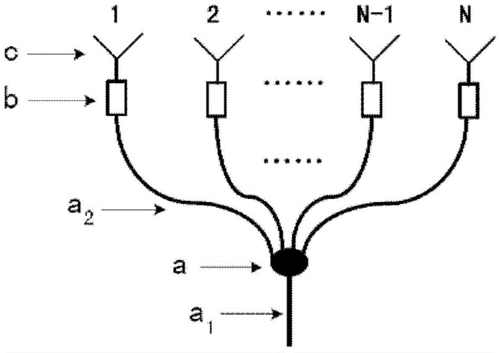
[0029] see figure 1 as shown, figure 1 It is a schematic diagram of a THz antenna array based on an InP-based optical mixer according to an embodiment of the present invention, including an input waveguide a1, a 1×N optical splitter a, N optical mixers b, and connecting N optical mixers b and optical splitters N passive waveguides a2 and N THz antennas c of a.

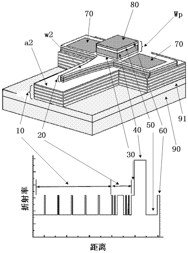
[0030] figure 2 It is a structural diagram of the unit mixer b of the THz antenna array based on the InP-based optical mixer according to the embodiment of the present invention. Fabricate a THz array. On the InP substrate 90, a buffer layer 91 and a passive waveguide layer 10 are successively grown. The passive waveguide layer 10 can be composed of InP layers (low refractive index layers) and InGaAsP layers with multiple cycles (the number of cycles in this embodiment is 5). Layers (high refractive index layers) are alternately composed, and may be composed of InGaAsP material alone. An optical coupling layer 20 ...

Embodiment 2

[0038] see Figure 5 , the implementation of the second embodiment is basically the same as that of the first embodiment, and the difference with the first embodiment is that the electrode d is made on the upper part of the passive waveguide a2 of the array, and the effective refractive index of the material of the waveguide layer 10 can be changed by current injection, thereby changing The optical path difference of the pump light between each mixer unit b constitutes a staring THz antenna array.


PUM


Abstract

The utility model discloses a manufacturing method of a THz antenna array. The method includes the following steps: 1) selecting a substrate; 2) sequentially growing materials of a buffer layer, a passive waveguide layer, an optical coupling layer, a refractive index matching layer, a light absorption layer, a cladding layer and a contact layer on the substrate; 3) sequentially etching the materials of the the contact layer, cladding layer, the light absorption layer, and the refractive index matching layer to the optical coupling layer, wherein the shape formed by the etching is a quadrilateral structure which is a photomixer waveguide; 4) manufacturing an electrode on the contact layer on the photomixer waveguide and manufacturing electrodes on the optical coupling layer at the two sides of the photomixer waveguide; 5) etching the optical coupling layer to a depth of reaching the passive waveguide layer so that a wedge optical coupling waveguide is formed; 6)etching the passive waveguide layer to the buffer layer so that a 1*N optical splitter, an input waveguide and a passive waveguide are formed and thus a substrate is formed; 7) manufacturing THz antennae on the substrate and finishing the preparation. The manufacturing method is capable of obtaining a high-performance THz antenna array device.

Description

technical field [0001] The invention relates to the field of optoelectronic devices, in particular to a method for manufacturing a THz antenna array. Background technique [0002] The frequency is 0.1-10THz (1THz=10 12 Hz) range are called terahertz (THz) waves. Due to its special position in the electromagnetic spectrum, THz waves are widely used in basic research fields such as physics, chemistry, astronomy, life science and medical science, as well as in security inspection, medical imaging, environmental monitoring, food inspection, radio astronomy, wireless communication and weapon guidance. And other applied research fields have great scientific research value and broad application prospects. The generation of THz waves is the key to the development and application of THz science and technology. Among the many types of THz sources, the THz source based on semiconductor optical mixing devices has the advantages of low cost, compact structure, and room temperature ope...

Claims


Application Information

Patent Timeline
Patent Type & Authority Patents(China)
IPC IPC(8): H01Q21/00G02B6/125
Inventor 梁松朱洪亮
Owner INST OF SEMICONDUCTORS - CHINESE ACAD OF SCI
Why Eureka
Try Eureka