Epitaxial production method capable of effectively improving P-GaN hole injection layer quality

A technology of hole injection layer and production method, which is applied in the direction of electrical components, circuits, semiconductor devices, etc., can solve the problems of device luminous performance degradation, low hole concentration, and difficult activation, so as to improve antistatic ability and luminous brightness , Improve the effect of activation efficiency

Inactive Publication Date: 2015-01-28
SUZHOU NANOJOIN PHOTONICS
View PDF5 Cites 11 Cited by
  • Summary
  • Abstract
  • Description
  • Claims
  • Application Information

AI Technical Summary

Problems solved by technology

However, considering that during the epitaxy process of the LED device structure, the InGaN/GaN multi-quantum active layer is grown in a low-temperature environment of 700-900°C, the subsequent high-temperature environment of p-GaN will inevitably cause serious damage to the InGaN active layer. Decomposition and segregation of In, and finally the luminous performance of the device is greatly reduced
However, when the p-GaN layer is grown at low temperature, it is difficult for Mg atoms to be incorporated into the GaN lattice.
At the same time, due to the deep position of the acceptor energy level of Mg, the activation is difficult, resulting in a relatively low hole concentration. In order to obtain the ideal hole concentration, a large flow of Mg is required.
When Mg is more, in addition to replacing

Method used


Image

  • Epitaxial production method capable of effectively improving P-GaN hole injection layer quality

Examples


Embodiment Construction

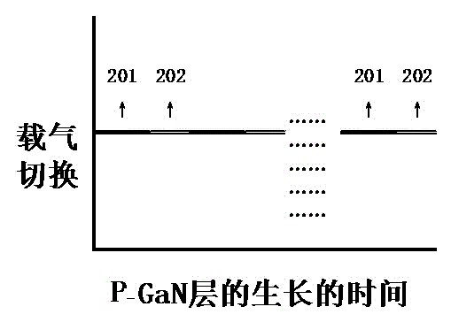
[0024] like figure 1 As shown, the present invention discloses an epitaxial production method that can effectively improve the quality of the p-GaN hole injection layer, using MOCVD technology, using NH3, TMGa or TEGa, TMIn, TMAl as N source, Ga source, In source and Al source, using Cp 2 Mg and SiH 4 As the dopant source of Mg and Si, similar to the existing method, the method comprises the following steps:

[0025] First, grow a GaN low-temperature buffer layer with a thickness of 25nm on the substrate, with H 2 As a carrier gas, the growth temperature is 450-650°C and the pressure is 50-1000mbar.

[0026] Then, the temperature is raised to grow an unintentionally doped GaN layer with a thickness of 1.5 μm on the GaN low-temperature buffer layer at a growth temperature of 850-1200° C. and a pressure of 50-1000 mbar.

[0027] Next, an n-GaN electron injection layer with a thickness of 2.5 μm is grown on the unintentionally doped GaN layer. Using SiH 4 Doping, the dopin...


PUM

PropertyMeasurementUnit
Thicknessaaaaaaaaaa

Abstract

The invention discloses an epitaxial production method capable of effectively improving P-GaN hole injection layer quality. The epitaxial production method capable of effectively improving the P-GaN hole injection layer quality includes the step of sequentially growing a low temperature GaN buffer layer, an unintentional doped GaN layer, an n type electron injection layer, a multiple quantum well active area, a p-GaN hole injection layer and a p type heavy doped contact layer on a substrate, wherein the P-GaN hole injection layer is grown in alternate type nitrogen and hydrogen carrier gas switching environment, doping of magnesium atoms is performed in nitrogen environment, and activation energy of the magnesium atoms is reduced in hydrogen environment. The P-GaN hole injection layer grown in the alternate type carrier gas switching environment can effectively improve efficiency of merging the magnesium atoms into GaN crystal lattices, improves quality of the GaN crystal lattices, reduces work voltage and improves antistatic ability. Simultaneously, activation efficiency of the magnesium atoms is improved, a large quantity of hole carriers are provided, and luminance of LED (light emitting diode) devices is improved by reducing the activation energy of the magnesium atoms.

Description

technical field [0001] The invention belongs to the field of LED epitaxial technology growth, in particular to a method for growing a high-quality p-GaN hole injection layer, which is suitable for the production of high-brightness GaN-based LED epitaxial wafers. Background technique [0002] As a solid-state light source, LED has the advantages of small size, high efficiency, long life, and environmental protection. It is known as the third-generation green energy-saving light source. Although LED has entered the stage of commercial production, in order to further improve the photoelectric performance of LED devices, in There are still many technical difficulties. [0003] One of the main problems is the growth of p-GaN layers of high quality and high hole concentration. In order to ensure the quality of the material and the activation rate of the dopant Mg, the growth temperature of the p-GaN material is generally above 1000°C. However, considering that during the epitaxy...

Claims


Application Information

Patent Timeline
IPC IPC(8): H01L33/00H01L33/14
CPCH01L33/025H01L33/06H01L33/14H01L33/145H01L2933/0033
Inventor 孔静蔡金冯美鑫南琦王辉王怀兵
Owner SUZHOU NANOJOIN PHOTONICS
Why Eureka
Try Eureka