Structure of MIS capacitor with capacitance being variable and manufacturing method thereof

A technology with variable capacitance value, applied in the manufacturing of circuits, electrical components, semiconductor/solid-state devices, etc., can solve the problems of power amplifier output power, gain and efficiency reduction, inability to match the working voltage range of power amplifiers, and inability to match all of them. Achieve the effect of increasing output power, reducing difficulty, and reducing nonlinearity

Active Publication Date: 2015-01-21
SHANGHAI HUAHONG GRACE SEMICON MFG CORP
View PDF3 Cites 1 Cited by
  • Summary
  • Abstract
  • Description
  • Claims
  • Application Information

AI Technical Summary

Problems solved by technology

[0002] In RFLDMOS process, Coss-V d curve like figure 1 As shown, it can be seen from the figure that the output capacitance will increase with the drain voltage V d If a capacitor with a voltage coefficient close to zero is connected in parallel at the output end at this time for internal matching, it will not be able to match the best value within the working voltage range of RFLDMOS, causing the power amplifier output power, gain and reduction in efficiency, etc.
[0003] The MIS capacitor usually used for internal matching uses silicon oxide or silicon nitride as the dielectric layer, and the substrate is a uniformly doped silicon substrate. The capacitance value will not change with the voltage change, so that the operating voltage of the power amplifier cannot range for the best fit

Method used


Image

  • Structure of MIS capacitor with capacitance being variable and manufacturing method thereof
  • Structure of MIS capacitor with capacitance being variable and manufacturing method thereof
  • Structure of MIS capacitor with capacitance being variable and manufacturing method thereof

Examples


Embodiment Construction

[0027] In order to have a more specific understanding of the technical content, characteristics and effects of the present invention, now in conjunction with the illustrated embodiment, the details are as follows:

[0028] The MIS capacitor applied in the RFLDMOS technology of the present invention, its specific manufacturing process is as follows:

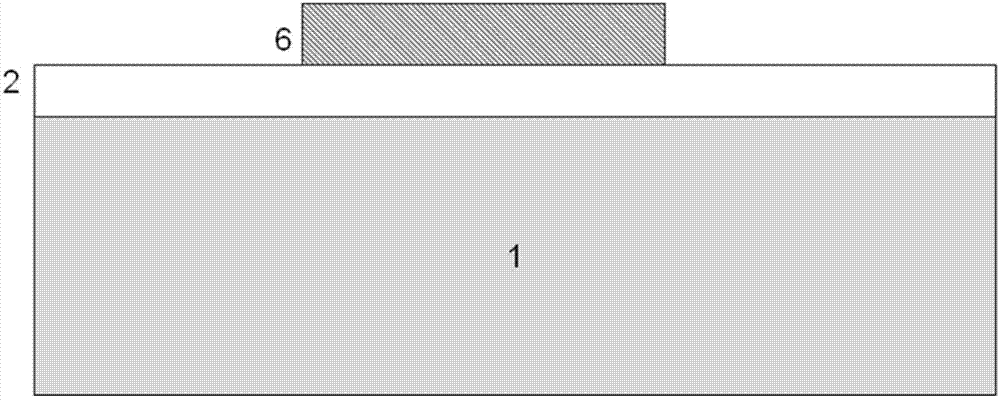
[0029] Step 1, grow N-type lightly doped silicon epitaxy 2 on N-type heavily doped silicon substrate 1, such as image 3 shown.

[0030] Step 2, grow a layer of silicon oxide 3 of about 100 Angstroms on the N-type lightly doped epitaxy 2 as a sacrificial oxide layer, such as Figure 4 shown.

[0031] Step 3, define an N-type ion implantation region through the photoresist 4, and perform vertical N-type ion implantation, such as Figure 5 shown. In this embodiment, phosphorous ions are implanted, the implantation energy is 30-100keV, and the implantation dose is 1e12-1e14cm -2 .

[0032] Step 4, perform the implantation of ph...


PUM


Abstract

The invention discloses a manufacturing method of an MIS capacitor with the capacitance being variable, which comprises the steps of 1) growing an N-type lightly doped epitaxy on an N-type heavily doped substrate; 2) growing a sacrificial oxidation layer; 3) defining an N-type ion implantation region and vertically implanting N-type ions; 4) implanting the N-type ions by an oblique angle; 5) removing a photoresist and carrying out thermal annealing; 6) removing the sacrificial oxidation layer and further depositing an oxidation layer; and 7) depositing a metal layer. The invention further discloses a structure of the MIS capacitor. A transverse wave-shaped concentration gradient of the implanted ions is formed in an N-type lightly doped epitaxial layer of the MIS capacitor through the vertical N-type ion implantation and the angled N-type ion implantation and diffusion after implantation. The structure enables the capacitance of the MIS capacitor to be increased along with increase in impressed voltage, the capacitance forms complementation with output capacitance of an RFLDMOS, and the nonlinearity of the output capacitance along with voltage can be reduced through parallel connection and internal matching of the MIS capacitor and the output capacitance of the RFLDMOS.

Description

technical field [0001] The invention relates to the field of semiconductor integrated circuit manufacturing, in particular to a structure and a manufacturing method of an MIS capacitor with variable capacitance applied to RFLDMOS technology. Background technique [0002] In RFLDMOS process, Coss-V d curve like figure 1 As shown, it can be seen from the figure that the output capacitance will increase with the drain voltage V d If a capacitor with a voltage coefficient close to zero is connected in parallel at the output end at this time for internal matching, it will not be able to match the best value within the working voltage range of RFLDMOS, causing the power amplifier output power, gain and reduction in efficiency, etc. [0003] MIS capacitors usually used for internal matching use silicon oxide or silicon nitride as the dielectric layer, and the substrate is a uniformly doped silicon substrate. The capacitance value will not change with the change of voltage, so th...

Claims


Application Information

Patent Timeline
Patent Type & Authority Applications(China)
IPC IPC(8): H01L21/334H01L21/266H01L29/94
CPCH01L21/266H01L29/66174H01L29/93
Inventor 蔡莹
Owner SHANGHAI HUAHONG GRACE SEMICON MFG CORP
Why Eureka
Try Eureka