A kind of industrialized preparation method of intelligent glass with automatic adjustment of infrared transmittance
A technology of infrared transmittance and automatic adjustment, which is applied in the fields of color preparation, doping, and PVD deposition. It can solve problems such as the industrial application of vanadium dioxide-based smart glass, meet market needs, and speed up circulation. , to achieve the effect of color change
- Summary
- Abstract
- Description
- Claims
- Application Information
AI Technical Summary
Problems solved by technology
Method used
Image
Examples
preparation example Construction
[0029] An industrialized preparation method for intelligent glass with automatic adjustment of infrared transmittance, the steps are as follows:
[0030] (1) Preparation of crystallization-inducing layer on glass surface
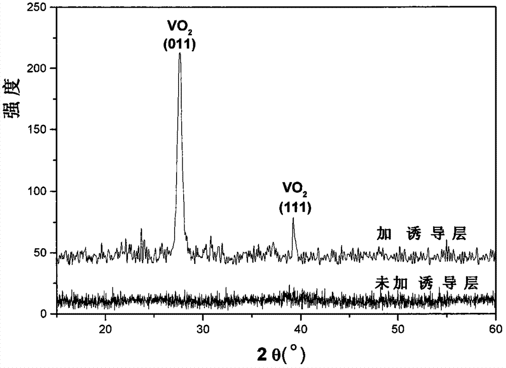
[0031] After the glass is routinely cleaned, a 5-20nm thick Ti or Si elemental film is sputtered and deposited on the glass surface by ion beam sputtering as a crystallization induction layer; or chemical vapor deposition is used on the cleaned glass surface ( PECVD) method deposits SiNx thin film of 40~80nm, as crystallization induction layer;
[0032] (2) Deposition of Vanadium Oxide Thin Film by DC Reactive Magnetron Sputtering
[0033] Using the DC reactive magnetron sputtering method, the vanadium oxide film is deposited on the crystallization induction layer by reactive sputtering; the reactive sputtering target is made of high-purity vanadium with a purity of 99.96% and doping elements with different atomic ratios; reactive sputtering Radiation sour...
Embodiment 1
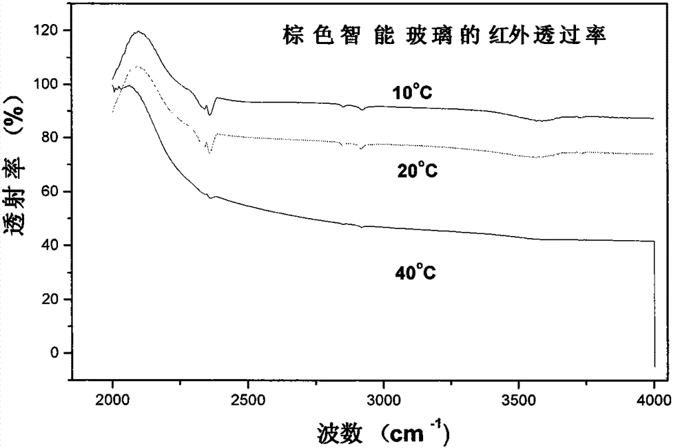
[0037] Embodiment 1 Brown smart glass preparation
[0038] 1. Preparation of crystallization-inducing layer on glass surface
[0039] After routine glass cleaning, chemical vapor deposition (PECVD) is used to deposit 70nm thick silicon-rich silicon nitride at 200°C as a crystallization induction layer, and its refractive index is 2.07;
[0040] 2. DC reactive magnetron sputtering vanadium oxide film deposition
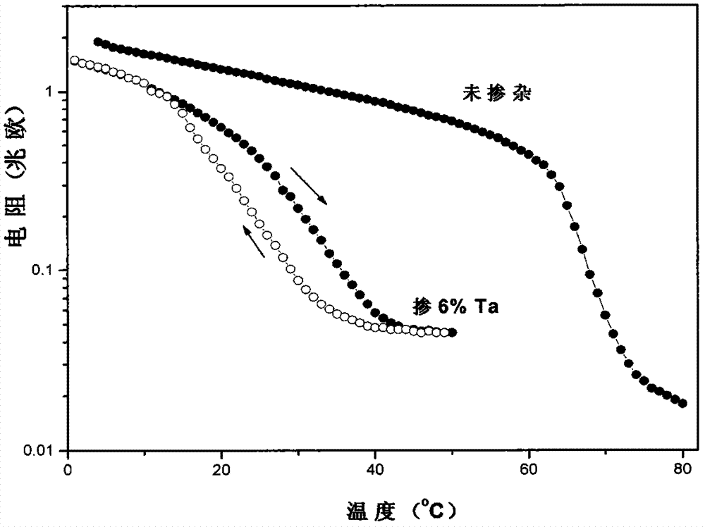
[0041] Using the DC reactive magnetron sputtering method, the vanadium oxide film was deposited on the crystallization induction layer by reactive sputtering; the reactive sputtering target was purchased 94% high-purity (99.96%) V and Ta with an atomic ratio of 6%. (purity 99.99%) molten alloy target. Reactive sputtering source gas is Ar / O 2 Mixed gas, Ar / O 2 The flow ratio is 8%, and the background vacuum of the sputtering chamber is 5×10 -4 Pa, the working vacuum degree during sputtering is 0.5Pa. During sputtering, a negative bias of 200V was applied to the sa...
Embodiment 2
[0045] Example 2 Preparation of blue smart glass
[0046] 1. Preparation of crystallization-inducing layer on glass surface
[0047] After the glass is routinely cleaned, use the ion beam sputtering method to deposit Ti with a purity of 99.99% on the glass surface with Ar ion sputtering, the sputtering acceleration voltage is 1500V, and the ion beam density is 0.4mA / cm 2 , the working vacuum degree is 1Pa, the sputtering deposition time is 5 minutes, and the thickness of the deposited Ti crystallization induction layer is about 10nm.
[0048] 2. DC reactive magnetron sputtering vanadium oxide film deposition
[0049] A direct current reactive magnetron sputtering method is used to deposit a vanadium oxide film on the crystallization induction layer by reactive sputtering; the deposited vanadium oxide film is a doped vanadium oxide film with a thickness of 180nm. The target material for reactive sputtering is a molten alloy target of 96% V (99.96% purity) and 1% La plus 3% Pd...
PUM
| Property | Measurement | Unit |
|---|---|---|
| phase transition temperature | aaaaa | aaaaa |
| electrical resistance | aaaaa | aaaaa |
| phase transition temperature | aaaaa | aaaaa |
Abstract
Description
Claims
Application Information
 - R&D
- Intellectual Property
- Life Sciences
- Materials
- Tech Scout
- Unparalleled Data Quality
- Higher Quality Content
- 60% Fewer Hallucinations
Browse by: Latest US Patents, China's latest patents, Technical Efficacy Thesaurus, Application Domain, Technology Topic, Popular Technical Reports.
© 2025 PatSnap. All rights reserved.Legal|Privacy policy|Modern Slavery Act Transparency Statement|Sitemap|About US| Contact US: help@patsnap.com


