
Patsnap Eureka
For R&D, Patsnap Eureka makes reading and utilizing patents & technical documents easy.
Patsnap Eureka AIR
Designed for self-driven R&D workflows. Generate viable solutions, solve complex R&D challenges, empower your innovation with AI.

Patsnap Eureka Materials
Designed for material experts only. Revolutionize your material R&D, from search, analyze, to developing new materials.

TechResearch
Generate reliable direction feasibility study reports for your R&D in just a few steps.

TechSeek
Discover and master advanced knowledge NOW. Basics, ideas, possibilities, all at once.

TechMind
As an expert in R&D Theories, TechMind can generates customized viable solutions instantly.

TechRisk
Analyze your overall solution with one click, know your potential R&D risks in advance.

TechMonitor
Get weekly tech updates, stay abreast of the latest tech innovations and key insights.
Method for manufacturing thin film transistor and thin film transistor
A technology of thin-film transistors and polysilicon layers, which is applied in the manufacture of transistors, semiconductor devices, semiconductor/solid-state devices, etc., to achieve the effect of simplifying the manufacturing process and satisfying precise control
- Summary
- Abstract
- Description
- Claims
- Application Information
AI Technical Summary
Problems solved by technology
Method used
Image

Examples
Embodiment Construction
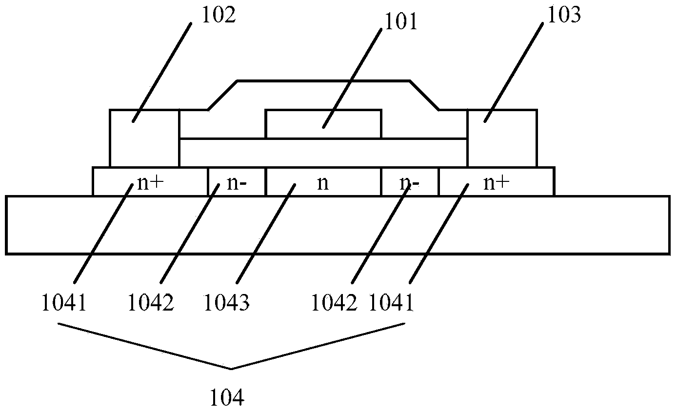
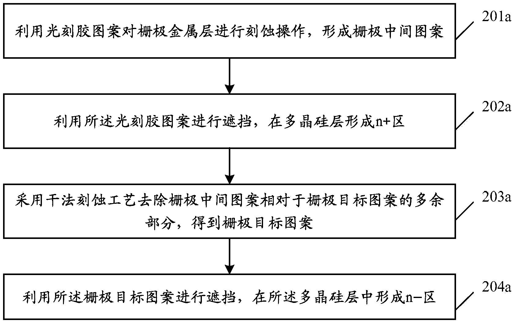
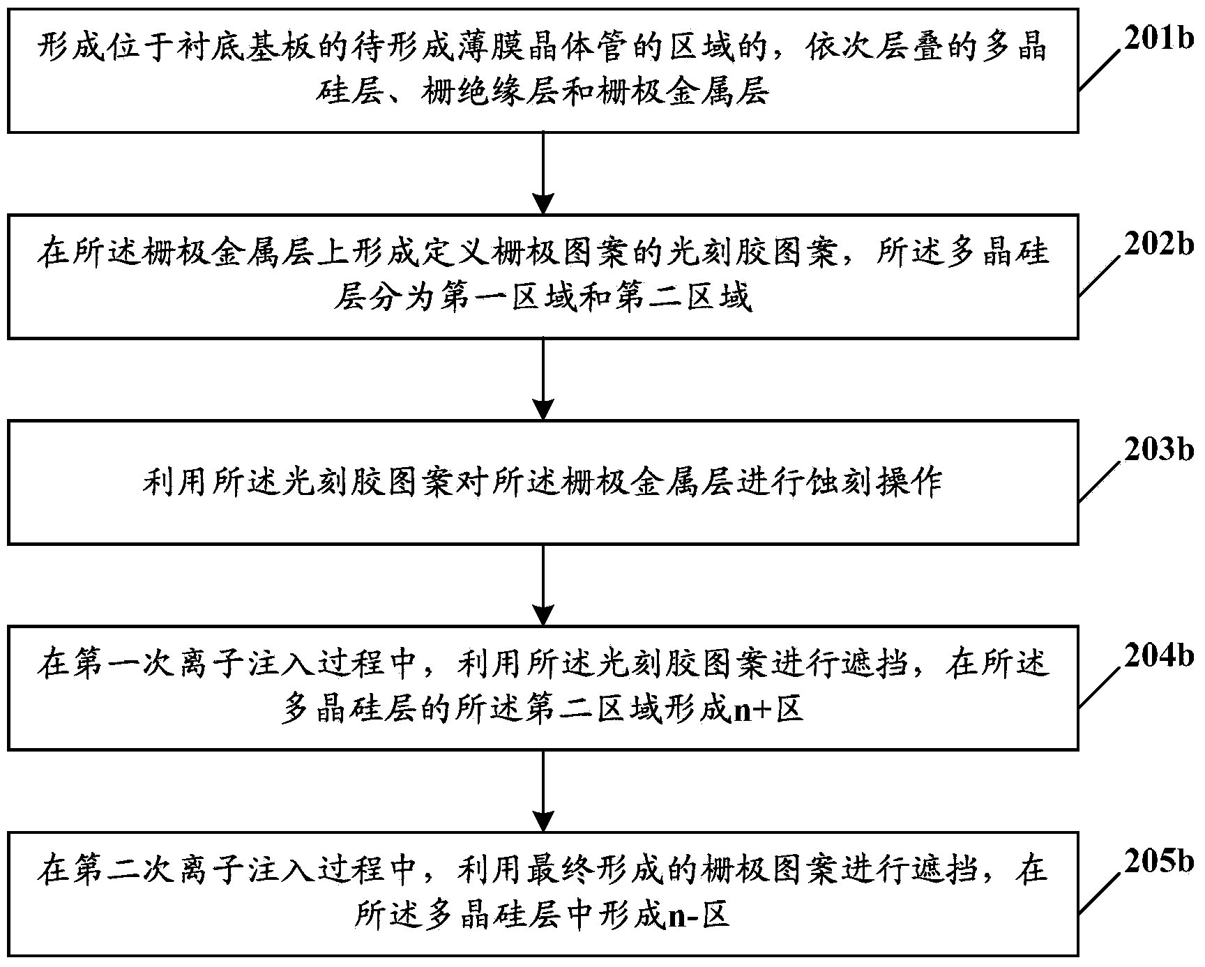
[0041] In the embodiment of the present invention, when forming the n+ region and n- region of the LTPS TFF, the above-mentioned n+ region and n- region are formed by using the photoresist defining the gate pattern and the gate target pattern as shields respectively. The resist precision and gate target pattern precision are controllable, so that the precision of the n-region can meet the precise control of the LDD structure size of the low-temperature polysilicon thin film transistor, and simplify the manufacturing process of the LTPS TFF.
[0042] Before the method of the embodiment of the present invention is described in detail, several process flows involved in the embodiment of the present invention are briefly described, so as to better understand the embodiment of the present invention.
[0043] In semiconductor manufacturing, it is necessary to use selected images, graphics or objects to block the film layer to be processed in order to control the active area of etch...
PUM
 Abstract
Description
Claims
Application Information
 - R&D Engineer
- R&D Manager
- IP Professional
- Industry Leading Data Capabilities
- Powerful AI technology
- Patent DNA Extraction
Browse by: Latest US Patents, China's latest patents, Technical Efficacy Thesaurus, Application Domain, Technology Topic, Popular Technical Reports.
© 2024 PatSnap. All rights reserved.Legal|Privacy policy|Modern Slavery Act Transparency Statement|Sitemap|About US| Contact US: help@patsnap.com