
Formation method for double-shallow trench isolator

A technology of double shallow trench isolation and shallow trench, which is applied in the field of formation of double shallow trench isolation, can solve the problems of silicon crystal lattice damage, poor device performance, leakage current image degradation, etc., and achieve good morphology, Improved dimensional uniformity and prevents shape instability

Inactive Publication Date: 2014-12-10
GALAXYCORE SHANGHAI
View PDF3 Cites 6 Cited by
  • Summary
  • Abstract
  • Description
  • Claims
  • Application Information

AI Technical Summary

Problems solved by technology

Sources of dark current include impurities in the silicon wafer, which can damage the silicon crystal lattice due to manufacturing process technology and heat buildup in the pixel area
Excessive dark current can generate leakage current and cause image degradation and poor device performance

Method used


Image

  • Formation method for double-shallow trench isolator
  • Formation method for double-shallow trench isolator
  • Formation method for double-shallow trench isolator

Examples


Embodiment Construction

[0029] As mentioned in the background art, the shallow trench isolation used in the pixel area is inconsistent with the depth of the shallow trench isolation in the logic area.

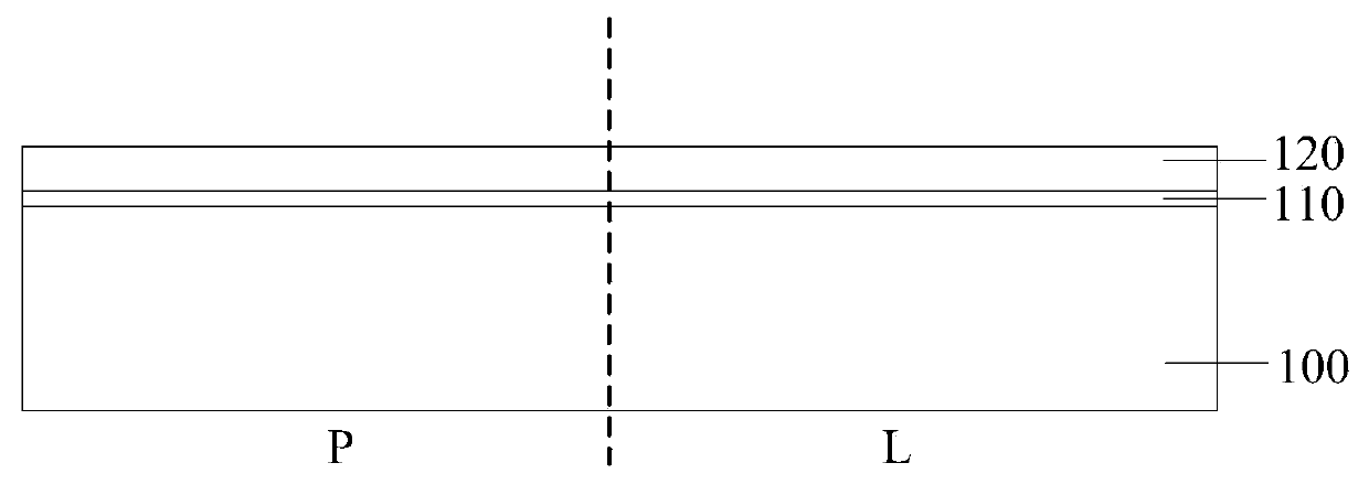
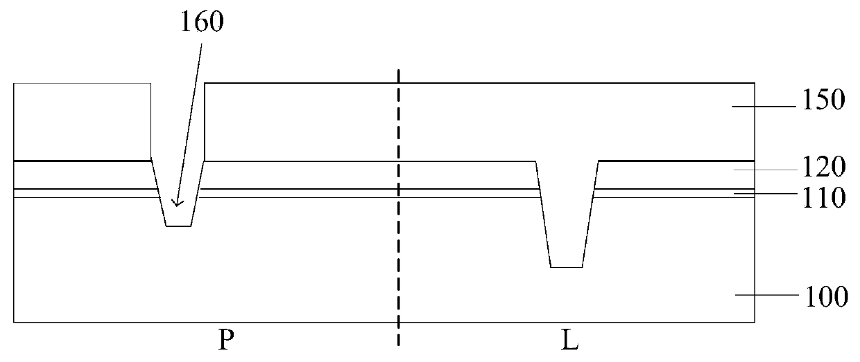
[0030] In order to make the corresponding double shallow trench isolation, an existing method such as Figures 1 to 4 shown.

[0031] Please refer to figure 1 , a substrate 100 is provided, and the substrate 100 includes a pixel region P and a logic region L. A silicon oxide layer 110 is formed on the substrate 100 , and a silicon nitride layer 120 is formed on the silicon oxide layer 110 .

[0032] Please refer to figure 2 , forming a first photoresist layer 130 on the silicon nitride layer 120, performing processes such as exposure and development on the first photoresist layer 130 to form an opening (not marked) on the logic region L, and using the first photoresist layer 130 with the opening A photoresist layer 130 is used as a mask to etch the silicon nitride layer 120, silicon oxide layer ...


PUM


Abstract

A formation method for double-shallow trench isolator includes that an oxide layer and a hard mask layer are formed on the surface of a substrate, and the substrate is provided with a first area and a second area; the hard mask layer and the oxide layer on the first area and the second area are etched till the surface of the substrate is exposed, the exposed surface of the first area forms a first part area, and the exposed surface of the second area forms a second part area; the hard mask layer is a mask, the first part area is etched to form a first shallow trench, and the second part area is etched to form a second shallow trench; the second shallow trench is protected, and the mask is taken as the hard mask layer to have the first shallow trench further etched to form a third shallow trench. By the formation method, the double-shallow trench is stable in isolation shape, high in uniformity and good in feature.

Description

technical field [0001] The invention relates to the field of semiconductor manufacturing, in particular to a method for forming double shallow trench isolation. Background technique [0002] CMOS image sensors (CMOS image sensors, CIS) are used in applications including digital cameras. In semiconductor technology, CIS is used to sense light projected onto a semiconductor substrate. Generally, these devices utilize an array of active pixels (ie, image sensing elements or cells) that include photodiodes and other elements (eg, transistors) to convert images into digital data or electrical signals. [0003] CIS products usually include a pixel area and a logic (circuit) area. Shallow trench isolation (STI) is a characteristic feature of integrated circuits, used to prevent leakage current between adjacent semiconductor components. [0004] Dark current is the harmful current generated by the pixel when it is not illuminated. The signal corresponding to the dark current may...

Claims


Application Information

Patent Timeline
Patent Type & Authority Applications(China)
IPC IPC(8): H01L21/762H01L27/146
CPCH01L21/76229H01L27/1463H01L27/14683
Inventor 王永刚李杰
Owner GALAXYCORE SHANGHAI
Learn More