Organic light emitting device and manufacturing method thereof
An electroluminescent device and electroluminescent technology, which can be applied in the fields of electro-solid devices, semiconductor/solid-state device manufacturing, electrical components, etc., and can solve problems such as low luminous efficiency
- Summary
- Abstract
- Description
- Claims
- Application Information
AI Technical Summary
Problems solved by technology
Method used
Image

Examples
preparation example Construction
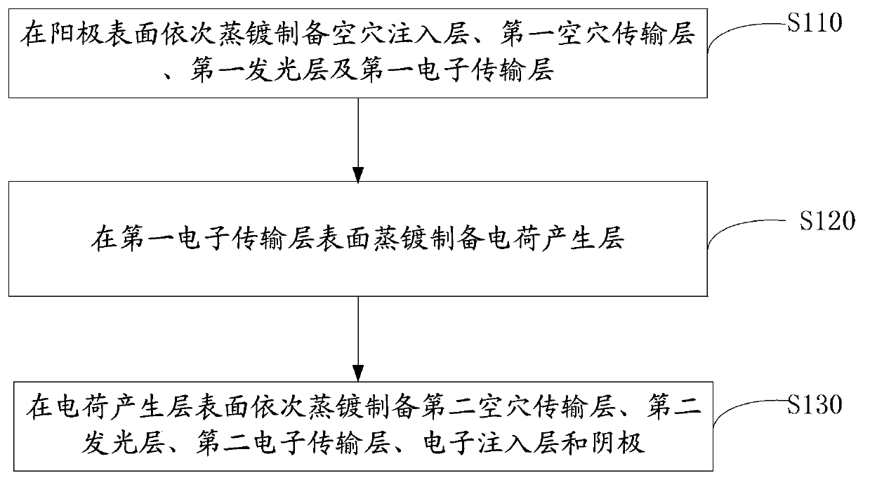
[0036] Please also see figure 2 , the preparation method of the organic electroluminescent device 100 of an embodiment, it comprises the following steps:
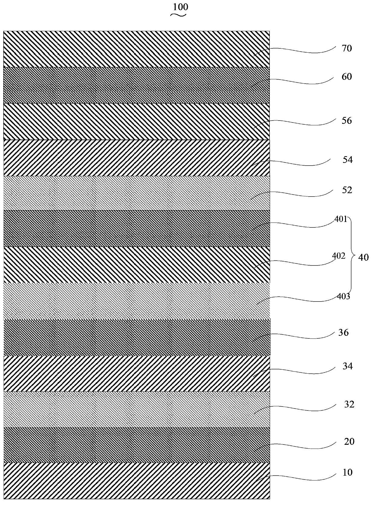
[0037] Step S110 , sequentially vapor-depositing the hole injection layer 20 , the first hole transport layer 32 , the first light emitting layer 34 and the first electron transport layer 36 on the surface of the anode.
[0038] The anode 10 is indium tin oxide glass (ITO), aluminum zinc oxide glass (AZO) or indium zinc oxide glass (IZO), preferably ITO.
[0039] In this embodiment, before the hole injection layer 20 is formed on the surface of the anode 10, the anode 10 is pretreated. The pretreatment includes: performing photolithography on the anode 10, cutting it into the required size, using detergent, deionized Water, acetone, ethanol, and isopropanone were each ultrasonically cleaned for 15 minutes to remove organic pollutants on the surface of the anode 10 .
[0040] The hole injection layer 20 is formed on the s...
Embodiment 1
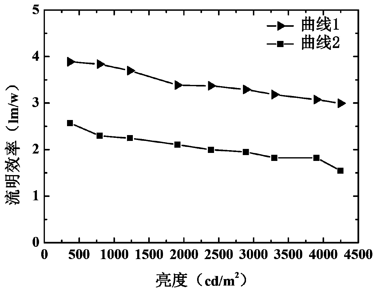
[0056] The structure prepared in this example is ITO / V 2 o 5 / NPB / BCzVBi / TPBI / MoO 3 / WO 3 : Ta 2 o 5 / PrO 2 / TAPC / BCzVBi / Bphen / CsF / Al organic electroluminescent device. Wherein, " / " indicates a stacked structure, and ":" indicates doping or mixing, and the following embodiments are the same.
[0057] First carry out photolithography treatment on ITO, cut it into the required size, and then use detergent, deionized water, acetone, ethanol, and isopropanol to sonicate for 15 minutes each to remove organic pollutants on the glass surface; evaporate the hole injection layer , the material is V 2 o 5 , with a thickness of 40nm; vapor-deposited the first hole transport layer, made of NPB, with a thickness of 25nm; vapor-deposited the first light-emitting layer, made of BCzVBi, with a thickness of 20nm; 60nm; evaporated charge generation layer, n-type layer is MoO 3 , the thickness is 20nm, the middle layer material is WO 3 : Ta 2 o 5 , WO 3 with Ta 2 o 5 The mass rat...
Embodiment 2
[0062] The structure prepared in this example is AZO / MoO 3 / TCTA / ADN / TAZ / V 2 o 5 / MoO 3 :Nb 2 o 5 / Pr 2 o 3 / NPB / ADN / TAZ / CsN 3 / Pt organic electroluminescent devices.
[0063] First, the AZO glass substrate was washed with detergent, deionized water, and ultrasonic for 15 minutes to remove organic pollutants on the glass surface; the hole injection layer was prepared by evaporation, and the material was MoO 3 , the thickness is 80nm; the first hole transport layer is prepared by evaporation, the material is TCTA, and the thickness is 60nm; the first light-emitting layer is prepared by evaporation, the material is ADN, and the thickness is 5nm; the first electron transport layer is prepared by evaporation, and the material is TAZ, the thickness is 200nm; evaporated charge generation layer, n-type layer is V 2 o 5 , the thickness is 10nm, and the material of the middle layer is MoO 3 :Nb 2 o 5 , MoO 3 with Nb 2 o 5 The mass ratio is 1:20, the thickness is 30nm, a...
PUM
 Abstract
Description
Claims
Application Information
 - R&D
- Intellectual Property
- Life Sciences
- Materials
- Tech Scout
- Unparalleled Data Quality
- Higher Quality Content
- 60% Fewer Hallucinations
Browse by: Latest US Patents, China's latest patents, Technical Efficacy Thesaurus, Application Domain, Technology Topic, Popular Technical Reports.
© 2025 PatSnap. All rights reserved.Legal|Privacy policy|Modern Slavery Act Transparency Statement|Sitemap|About US| Contact US: help@patsnap.com