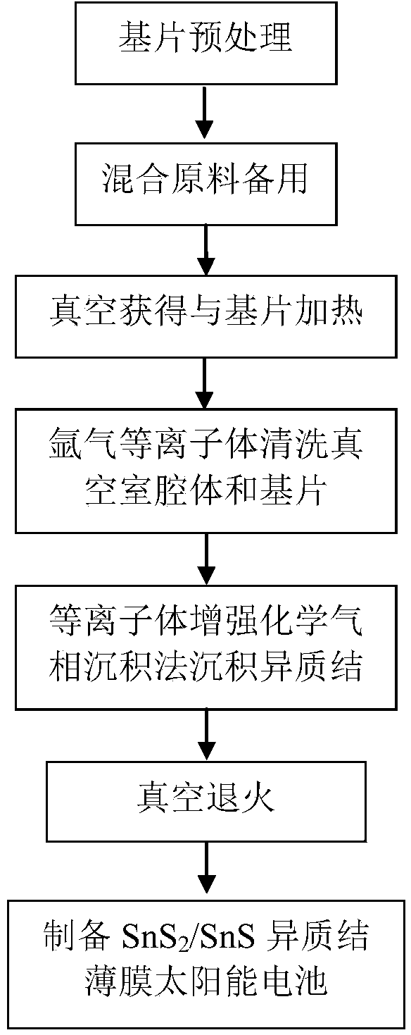
Method for manufacturing SnS2/SnS heterojunction thin-film solar cell at a time
A solar cell and heterojunction technology, applied in circuits, photovoltaic power generation, electrical components, etc., can solve the problems of poor bonding between p-type thin films and n-type thin films, large series resistance of solar cells, and increased production costs. The effect of shortening the production cycle, improving the photoelectric conversion efficiency, and simple method
- Summary
- Abstract
- Description
- Claims
- Application Information
AI Technical Summary
Problems solved by technology
Method used
Image
Examples
preparation example Construction
[0039] A kind of SnS 2 The one-time preparation method of / SnS heterojunction thin-film solar cell comprises the following steps:
[0040] (1) Wash the substrate successively with hydrochloric acid, sodium hydroxide, sulfuric acid, acetone, alcohol, and deionized water, and dry;
[0041] (2) Place the cleaned and dried substrate on the upper substrate in the vacuum chamber cavity of the plasma enhanced chemical vapor deposition (PECVD) system, and simultaneously fix the upper substrate and the lower substrate in the cavity;
[0042] (3) Put the mixed raw material containing tin element and sulfur element in the crucible according to a certain ratio, wherein the ratio of the amount of tin element and sulfur element in the mixed raw material is 1:2 to 1:5, and put the crucible into In the reaction source heating device of the plasma enhanced chemical vapor deposition system;
[0043] (4) Close the chamber of the plasma chemical vapor deposition system, turn on the mechanical pu...
Embodiment 1
[0061] (1) Clean the FTO conductive glass successively with hydrochloric acid, sodium hydroxide, sulfuric acid, acetone, alcohol, deionized water, and dry;
[0062] (2) Place the cleaned and dried substrate on the upper substrate of the plasma-enhanced chemical vapor deposition (PECVD) system, and simultaneously fix the upper substrate and the lower substrate in the cavity;
[0063] (3) Take by weighing 5.15g of sodium thiosulfate pentahydrate (Na 2 S 2 o 3 ·5H 2 O) and 5.40g of tin tetrachloride (SnCl 4 ) is placed in the crucible (the ratio of the amount of tin element to sulfur element is 1:2.005), and put into the reaction source heating device of the plasma enhanced chemical vapor deposition system together with the crucible;
[0064] (4) Close the cavity of the plasma chemical vapor deposition system, turn on the mechanical pump (primary pump), and when the pressure is pumped to 30Pa, turn on the molecular pump (secondary pump), and pump the pressure to 5×10 -2 Pa; ...
Embodiment 2
[0080] (1) Clean the FTO conductive glass successively with hydrochloric acid, sodium hydroxide, sulfuric acid, acetone, alcohol, deionized water, and dry;
[0081] (2) Place the cleaned and dried substrate on the substrate table (upper substrate) in the cavity of the plasma enhanced chemical vapor deposition (PECVD) system, and fix the upper substrate and the lower substrate in the cavity;
[0082] (3) Weigh 7.50g of sodium thiosulfate pentahydrate (Na 2 S 2 o 3 ·5H 2 O) and 4.30g of tin tetrachloride pentahydrate ((SnCl 4 ·5H 2 O) (the ratio of the amount of tin element to sulfur element is 1:4.933) is placed in the crucible, and put into the reaction source heating device of the plasma enhanced chemical vapor deposition system;
[0083](4) Close the cavity of the plasma chemical vapor deposition system, turn on the mechanical pump (primary pump), and when the pressure reaches 30Pa, turn on the molecular pump (secondary pump), and pump the pressure to 1×10 -2 Pa;
[0...
PUM
 Abstract
Description
Claims
Application Information
 - Generate Ideas
- Intellectual Property
- Life Sciences
- Materials
- Tech Scout
- Unparalleled Data Quality
- Higher Quality Content
- 60% Fewer Hallucinations
Browse by: Latest US Patents, China's latest patents, Technical Efficacy Thesaurus, Application Domain, Technology Topic, Popular Technical Reports.
© 2025 PatSnap. All rights reserved.Legal|Privacy policy|Modern Slavery Act Transparency Statement|Sitemap|About US| Contact US: help@patsnap.com


