Thin film transistor and production method thereof and array substrate

A technology of thin film transistor and manufacturing method, which is applied in transistors, semiconductor/solid-state device manufacturing, semiconductor device and other directions, can solve problems such as poor electrical contact between source and drain and oxide semiconductor layer, and achieves solving the problem of poor electrical contact and eliminating masking. Mold process forming process, good lattice matching effect

Active Publication Date: 2014-10-29
BEIJING BOE OPTOELECTRONCIS TECH CO LTD
View PDF10 Cites 10 Cited by
  • Summary
  • Abstract
  • Description
  • Claims
  • Application Information

AI Technical Summary

Problems solved by technology

[0017] In view of this, the main purpose of the present invention is to provide a thin film transistor and its manufacturing method and array substrate, which can effectively solve the problem of poor electrical contact between the source and drain electrodes and the oxide semiconductor layer

Method used


Image

  • Thin film transistor and production method thereof and array substrate
  • Thin film transistor and production method thereof and array substrate
  • Thin film transistor and production method thereof and array substrate

Examples


Embodiment Construction

[0063] The basic idea of ​​the present invention is: when forming the source and drain electrodes, directly deposit the highly doped amorphous silicon thin film on the oxide semiconductor thin film layers on both sides of the barrier layer to increase the carrier concentration at the oxide semiconductor interface, In this way, the oxide semiconductor can exhibit the electrical characteristics of a conductor, and the source and drain electrodes are formed.

[0064] The present invention will be described in further detail below in conjunction with the accompanying drawings and specific embodiments.

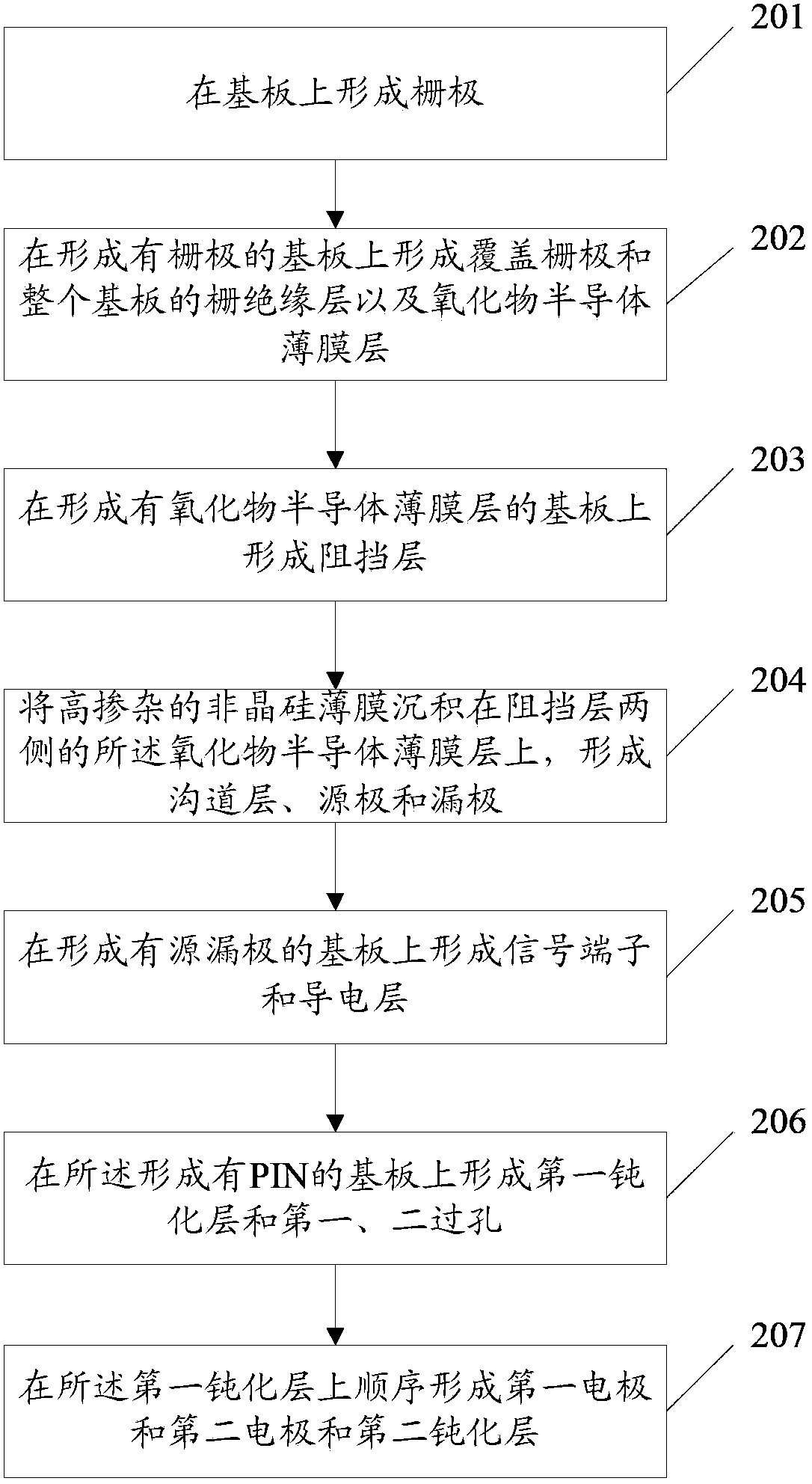
[0065] figure 2 It is a schematic flow chart of the manufacturing method of the thin film transistor of the present invention, such as figure 2 As shown, the implementation method is as follows:

[0066] Step 201: forming a gate on the substrate;

[0067] Specifically, a gate layer thin film is formed on the substrate 1 and patterned to form the gate 2 . Here, the gate can be...


PUM


Abstract

Provided are a thin film transistor, a method for manufactur thereof and an array substrate. The thin film transistor comprises: a gate electrode (102) formed on a substrate (101), a gate insulating layer (103) formed on the gate electrode (102) and covering at least a part of the substrate (101), and a semiconductor layer (105'), a source electrode (107a) and a drain electrode (107b) formed on the gate insulating layer (103). The material of the semiconductor layer (105') is an oxide semiconductor, and the material of the source electrode (107a) and the drain electrode (107b) is a doped oxide semiconductor. The source electrode (107a), the drain electrode (107b) and the semiconductor layer (105') are disposed in the same layer.

Description

technical field [0001] The invention relates to the technical field of displays, in particular to a thin film transistor, a manufacturing method thereof, and an array substrate. Background technique [0002] At present, oxide thin film transistors are mainly zinc oxide-based thin film field effect transistors of polycrystalline oxide semiconductor materials, and amorphous oxide semiconductors, such as: indium gallium zinc oxide (IGZO) semiconductors are used as the semiconductor layer of oxide thin film transistors. Its excellent properties such as high mobility, low sub-threshold, low current, and low-temperature production have attracted the attention of the liquid crystal industry. However, there are still some problems to be solved in the existing amorphous oxide semiconductor thin film transistors, for example, it is difficult to form a good electrical contact between the source and drain electrodes of the metal material and the amorphous oxide semiconductor layer. [...

Claims


Application Information

Patent Timeline
Patent Type & Authority Applications(China)
IPC IPC(8): H01L29/786H01L21/336H01L27/15
CPCH01L23/535H01L29/66969H01L29/786H01L29/78618H01L29/7869H01L2924/0002H01L29/78693H01L27/1225H01L2924/00
Inventor 阎长江龙君朱孝会谢振宇陈旭
Owner BEIJING BOE OPTOELECTRONCIS TECH CO LTD
Why Eureka
Try Eureka