
Multilayer ceramic electronic component and board for mounting the same

一种电子元件、多层陶瓷的技术,应用在电气元件、非印制电元件相联接的印刷电路、叠层电容器等方向,能够解决可靠性降低、倾倒等问题

Inactive Publication Date: 2014-10-29
SAMSUNG ELECTRO MECHANICS CO LTD
View PDF6 Cites 4 Cited by
  • Summary
  • Abstract
  • Description
  • Claims
  • Application Information

AI Technical Summary

Problems solved by technology

[0014] One aspect of the present invention provides a multilayer ceramic electronic component, which can prevent the reduction of reliability caused by steps, and can also solve the problem that occurs when a multilayer ceramic capacitor is mounted on a board such as a printed circuit board. dumping problem, and can achieve high-level capacitance by increasing the number of stacked layers

Method used


Image

  • Multilayer ceramic electronic component and board for mounting the same
  • Multilayer ceramic electronic component and board for mounting the same
  • Multilayer ceramic electronic component and board for mounting the same

Examples


Embodiment Construction

[0028] Hereinafter, embodiments of the present invention will be described in detail with reference to the accompanying drawings.

[0029] However, this invention may be embodied in many different forms and should not be construed as limited to the embodiments set forth herein. Rather, these embodiments are provided so that this disclosure will be thorough and complete, and will fully convey the scope of the invention to those skilled in the art.

[0030] In the drawings, the size and shape of components may be exaggerated for clarity, and the same reference numerals will be used throughout to designate the same or like components.

[0031] Hereinafter, a multilayer ceramic electronic component according to an embodiment of the present invention will be described, in particular, a multilayer ceramic capacitor will be described. However, the present invention is not limited thereto.

[0032] Multilayer Ceramic Capacitors

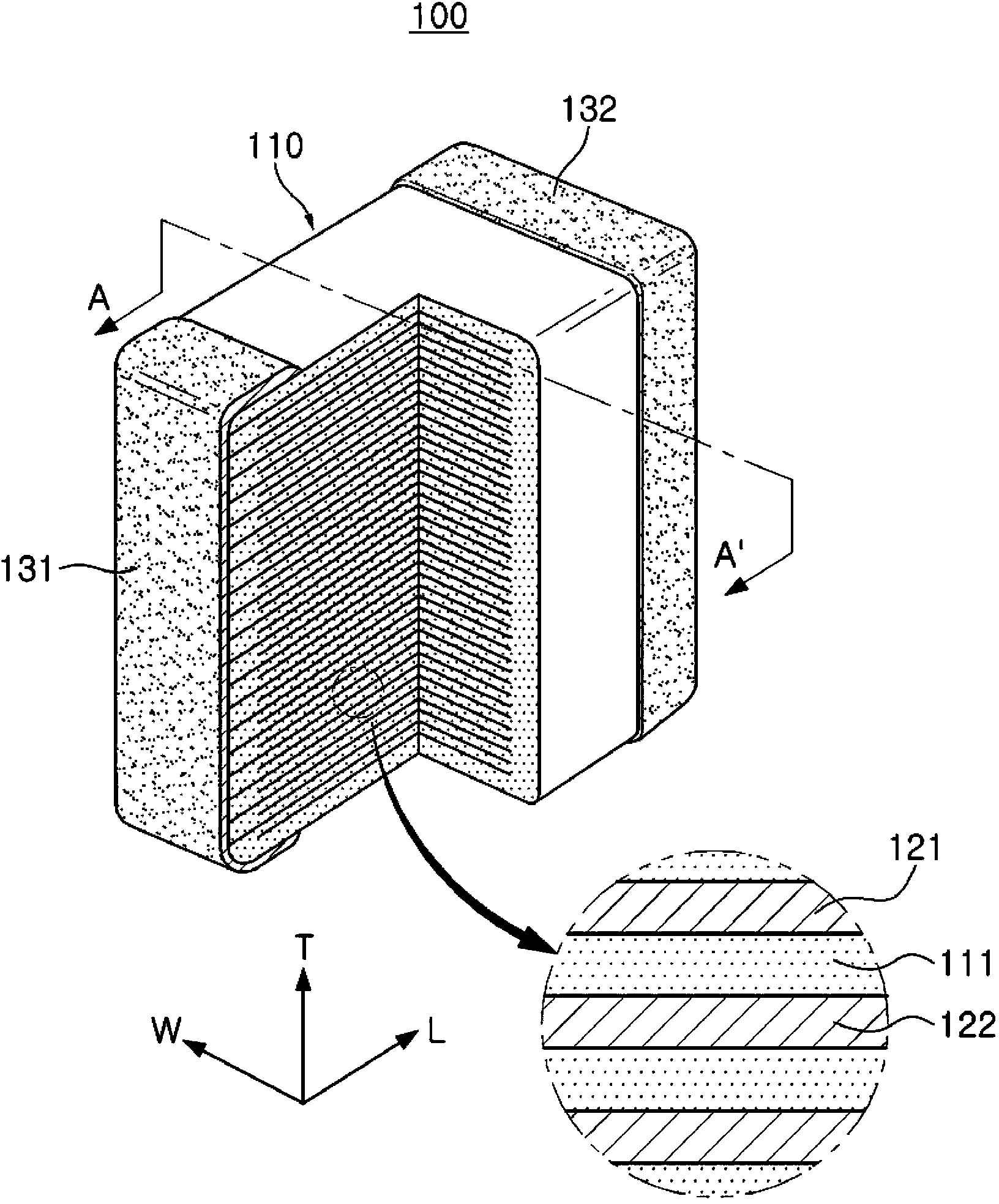
[0033] figure 1 is a partially cutaway perspectiv...


PUM


Abstract

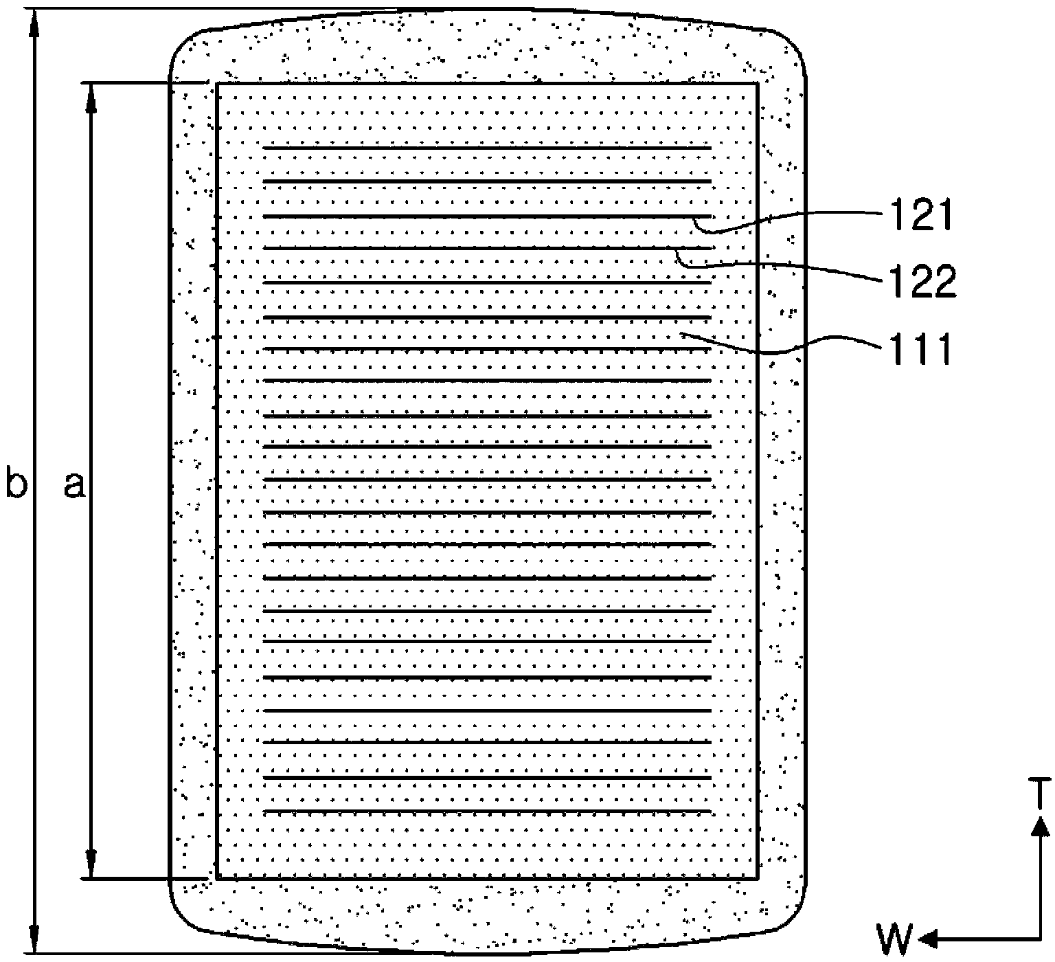
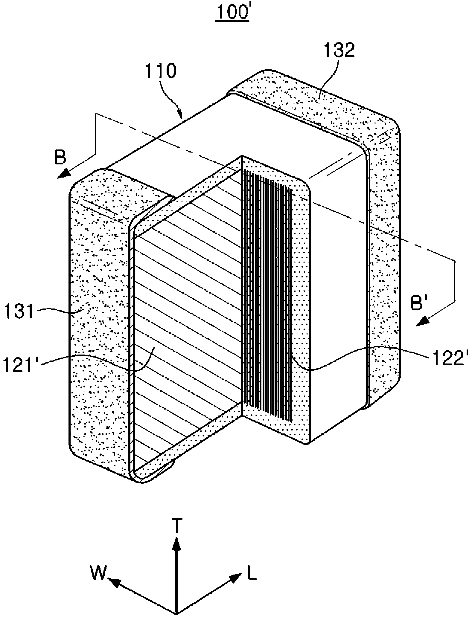
There is provided a multilayer ceramic electronic component includes: a ceramic body including dielectric layers stacked therein and satisfying T(thickness) / W(width)>1.0; first and second internal electrodes disposed to face each other in the ceramic body, having the dielectric layer disposed therebetween, and alternately exposed through end surfaces of the ceramic body; and first and second external electrodes extended from the end surfaces of the ceramic body to upper and lower main surfaces of the ceramic body wherein, when a height of the ceramic body is defined as a, and a distance from an upper end of the first or second external electrode formed on the upper main surface of the ceramic body to a lower end of the first or second external electrode formed on the lower main surface of the ceramic body is defined as b, 0.990≰a / b<1 is satisfied.

Description

[0001] Cross References to Related Applications [0002] This application claims priority from Korean Patent Application No. 10-2013-0046769 filed with the Korean Intellectual Property Office on Apr. 26, 2013, the contents of which are hereby incorporated by reference into this application. technical field [0003] The present invention relates to a multilayer ceramic electronic component and a board for mounting the multilayer ceramic electronic component. Background technique [0004] As electronic products tend to be miniaturized recently, multilayer ceramic electronic components used in electronic products need to be reduced in size and implemented with high-grade capacitance therein. [0005] Therefore, various methods have been tried in an attempt to stack a larger number of thin dielectric layers and internal electrodes, and recently, multilayer ceramic electronic components have been manufactured in which the thickness of the dielectric layer is reduced and the numbe...

Claims


Application Information

Patent Timeline
Patent Type & Authority Applications(China)
IPC IPC(8): H01G4/30H01G4/12H01G4/005H05K1/18
CPCH05K1/181H01G2/065H01G4/30H01G4/012H01G4/232H05K3/3442H05K2201/09381H05K2201/10015H05K2201/10636Y02P70/50H01G2/06H01G4/12
Inventor 韩丙禹小野雅章崔才烈金相赫
Owner SAMSUNG ELECTRO MECHANICS CO LTD
Learn More