A light-emitting diode with an anti-expansion layer and its manufacturing method

A technology of light-emitting diodes and manufacturing methods, which is applied in the direction of electrical components, circuits, semiconductor devices, etc., can solve the problems of epitaxial layer, oxide layer shedding, and poor connection, so as to avoid epitaxial layer shedding, structural connection stability, and improve external quantum luminescence efficiency effect

Active Publication Date: 2017-09-26
XIAMEN QIANZHAO SEMICON TECH CO LTD
View PDF13 Cites 0 Cited by
  • Summary
  • Abstract
  • Description
  • Claims
  • Application Information

AI Technical Summary

Problems solved by technology

However, the oxide layer is subsequently vapor-deposited on the epitaxial layer, and the connection with the epitaxial layer is poor, and there is a problem that the epitaxial layer and the oxide layer fall off easily.

Method used


Image

  • A light-emitting diode with an anti-expansion layer and its manufacturing method
  • A light-emitting diode with an anti-expansion layer and its manufacturing method
  • A light-emitting diode with an anti-expansion layer and its manufacturing method

Examples


Embodiment 1

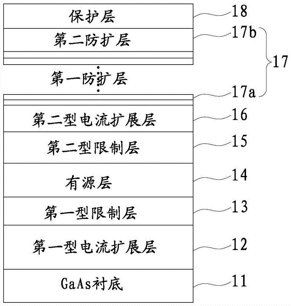
[0055] figure 1 As shown, the epitaxial structure of a light-emitting diode with an inverted structure disclosed in the present invention includes a GaAs substrate 11, and a first-type current spreading layer 12, a first-type confinement layer 13, and a Source layer 14, second-type confinement layer 15, second-type current spreading layer 16, anti-spreading layer 17, and protective layer 18, wherein the anti-spreading layer 17 is epitaxially formed by the first anti-spreading layer 17a and the second anti-spreading layer 17b Structure and composition.

[0056] Consists of a first-type current spreading layer 12 (N-type current spreading layer), a first-type confinement layer 13 (N-type confinement layer), an active layer 14, a second-type confinement layer 15 (P-type confinement layer), a second-type confinement layer The material of the current spreading layer 16 (P-type current spreading layer) is a group III-V compound such as AlGaInP. Specifically, the first-type current...

Embodiment 2

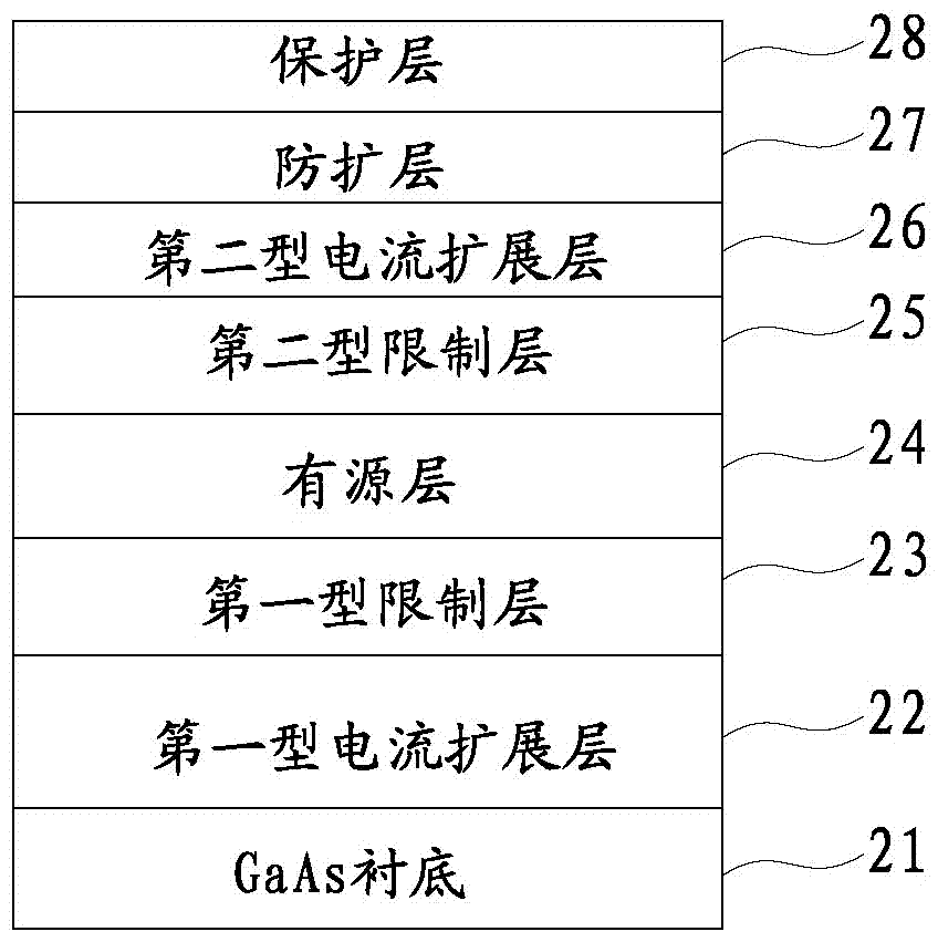
[0070] image 3 As shown, the epitaxial structure of an inverted light-emitting diode disclosed in the present invention includes a GaAs substrate 21, and along the upper surface of the GaAs substrate 21, a first-type current spreading layer 22, a second-type confinement layer 23, The active layer 24 , the second-type confinement layer 25 , the second-type current spreading layer 26 , the anti-spreading layer 27 and the protection layer 28 .

[0071] Consists of a first-type current spreading layer 22 (N-type current spreading layer), a first-type confinement layer 23 (N-type confinement layer), an active layer 24, a second-type confinement layer 25 (P-type confinement layer), a second-type confinement layer The material of the current spreading layer 26 (P-type current spreading layer) is a group III-V compound such as AlGaInP. Specifically, the first type current spreading layer 22 is made of (Al 0.35 Ga 0.65 ) 0.5 In 0.5 Composed of P material, the first-type confineme...


PUM

PropertyMeasurementUnit
thicknessaaaaaaaaaa
thicknessaaaaaaaaaa
thicknessaaaaaaaaaa

Abstract

The invention discloses a light-emitting diode (LED) with an anti-expansion layer and a manufacture method of the LED. In an earlier stage, the epitaxial growth anti-expansion layer is added; in a later-period diode manufacture process, a metal reflection mirror is formed over the anti-expansion layer, a metal electric conduction channel is embedded into the anti-expansion layer, the anti-expansion layer is changed into an oxide medium layer by means of an oxidation process, the oxide medium layer, the metal reflection mirror, and the electric conduction channel form a composite all-dimensional reflection effect, and two composite structures are formed by adding a bragg reflection layer to obtain high lighting brightness. By means of the method, problems that material interfaces of epitaxial layers, oxidation films, and metal reflection mirrors are easy to peel in an epitaxial layer evaporation oxidation film process in a traditional inverted chip manufacture process are solved, stability of the LED is improved, and a rate of finished products is increased. According to the LED with the anti-expansion layer and a manufacture method of the LED, external quantum efficiency is high, and connection of inner layer structures is stable.

Description

technical field [0001] The invention relates to the technical field of light-emitting diodes, in particular to a light-emitting diode with an anti-expansion layer and a manufacturing method thereof. Background technique [0002] In the prior art, high-brightness light-emitting diodes generally use a multiple quantum well structure as the active layer. Electrons and holes recombine in the quantum wells and release energy in the form of light, and the internal quantum efficiency reaches a relatively high level. high level. However, part of the light emitted from the quantum well will be directly absorbed by the substrate, and part of it will be reflected at the total reflection interface formed by the light-emitting diode and air or packaging material, and cannot be transmitted until it is absorbed inside, so the external quantum efficiency Still lower. Therefore, the light-emitting diode designed as an inverted structure can better reflect light by adding a metal reflector,...

Claims


Application Information

Patent Timeline
Patent Type & Authority Patents(China)
IPC IPC(8): H01L33/44H01L33/00
CPCH01L33/0062H01L33/10H01L33/44
Inventor 林志伟姜伟陈凯轩尧刚张永杨凯白继锋蔡建九刘碧霞
Owner XIAMEN QIANZHAO SEMICON TECH CO LTD
Why Eureka
Try Eureka