Substrate for power modules, substrate with heat sink for power modules, power module, method for producing substrate for power modules, and paste for bonding copper member
A technology of power modules and manufacturing methods, which is applied in semiconductor/solid-state device components, manufacturing tools, electric solid-state devices, etc., can solve the problems of ceramic substrate cracking, Ag-Cu eutectic structure layer hardness, etc., and achieve the effect of suppressing cracking
- Summary
- Abstract
- Description
- Claims
- Application Information
AI Technical Summary
Problems solved by technology
Method used
Image


Examples
no. 1 approach
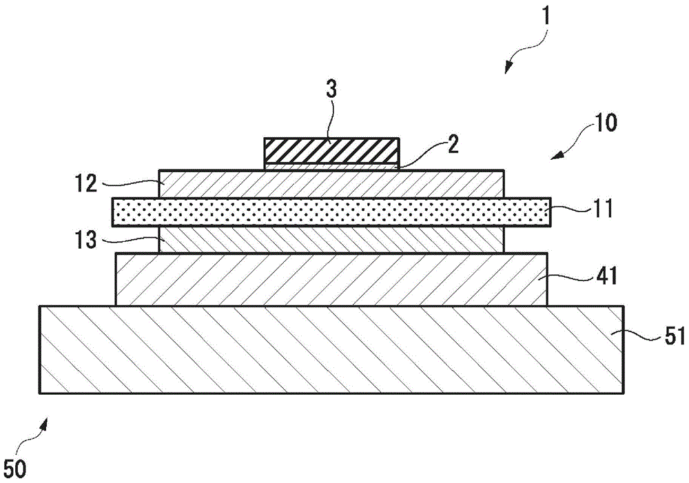
[0064] First, the first embodiment will be described. figure 1 In the figure, the power module substrate 50 with a heat sink and the power module 1 using the power module substrate 10 of this embodiment are shown.
[0065] This power module 1 includes a power module substrate 10 provided with a circuit layer 12 , a semiconductor element 3 (electronic component) bonded to the surface of the circuit layer 12 via a solder layer 2 , a buffer plate 41 , and a heat sink 51 . The solder layer 2 is, for example, Sn-Ag-based, Sn-In-based, or Sn-Ag-Cu-based solder. In this embodiment, a Ni plating layer (not shown) is provided between the circuit layer 12 and the solder layer 2 .
[0066] The power module substrate 10 includes a ceramic substrate 11, and is arranged on one surface of the ceramic substrate 11 ( figure 1 The circuit layer 12 in the middle is the upper surface), and the other surface of the ceramic substrate 11 ( figure 1 The middle is the metal layer 13 of the lower su...
no. 2 approach
[0137] Next, a second embodiment will be described. Figure 7 The middle table shows the power module substrate 110 of this embodiment. This power module substrate 110 includes a ceramic substrate 111, and is disposed on one surface of the ceramic substrate 111 ( Figure 7 The circuit layer 112 on the upper surface of the ceramic substrate 111 and the other surface of the ceramic substrate 111 ( Figure 7 The metal layer 113 in the lower surface).
[0138] The ceramic substrate 111 prevents electrical connection between the circuit layer 112 and the metal layer 113, and is made of highly insulating Si 3 N 4 (silicon nitride) composition. The thickness of the ceramic substrate 111 is preferably set within a range of 0.2 to 1.5 mm, and is set to 0.32 mm in the present embodiment.
[0139] Such as Figure 10 As shown, the circuit layer 112 is bonded to one side of the ceramic substrate 111 through a copper plate 122 ( Figure 10 The middle is the upper surface). The thick...
Embodiment
[0188] A comparative experiment performed to confirm the effectiveness of the present invention will be described. Various slurries were produced under the conditions shown in Table 1, Table 2, and Table 3. In Table 1, alloy powders were used as powder components. In Table 2, powders of respective elements (element powders) were used as powder components. In Table 3, powders of respective elements (element powders) were used as powder components, and hydride powders of nitride-forming elements were used as nitride-forming elements. In Table 3, in addition to the element powder mixing ratio of the hydride of the nitride-forming element, the content of the nitride-forming element (active metal content) is also described.
[0189] An anionic surfactant is used as a dispersant, dibutyl adipate is used as a plasticizer, and abietic acid is used as a reducing agent.
[0190] The mixing ratio of resin, solvent, dispersant, plasticizer, and reducing agent other than powder componen...
PUM
| Property | Measurement | Unit |
|---|---|---|
| thickness | aaaaa | aaaaa |
| thickness | aaaaa | aaaaa |
| particle diameter | aaaaa | aaaaa |
Abstract
Description
Claims
Application Information
 - R&D
- Intellectual Property
- Life Sciences
- Materials
- Tech Scout
- Unparalleled Data Quality
- Higher Quality Content
- 60% Fewer Hallucinations
Browse by: Latest US Patents, China's latest patents, Technical Efficacy Thesaurus, Application Domain, Technology Topic, Popular Technical Reports.
© 2025 PatSnap. All rights reserved.Legal|Privacy policy|Modern Slavery Act Transparency Statement|Sitemap|About US| Contact US: help@patsnap.com