Eureka AIR delivers breakthrough ideas for toughest innovation challenges, trusted by R&D personnel around the world.

Forming method of multigraph

A technology of multiple graphics and graphics, which is applied in the fields of electrical components, semiconductor/solid-state device manufacturing, circuits, etc., can solve the problems of complex process and high cost of small-sized multiple graphics, and achieve uniform width and spacing, uniform spacing, and film shape retention Good results

Inactive Publication Date: 2014-09-03
SEMICON MFG INT (SHANGHAI) CORP
View PDF4 Cites 19 Cited by
  • Summary
  • Abstract
  • Description
  • Claims
  • Application Information

AI Technical Summary

Problems solved by technology

[0014] The problem solved by the present invention is that the process of forming small-sized multiple patterns in the prior art is complicated and the cost is high

Method used


Image

  • Forming method of multigraph
  • Forming method of multigraph
  • Forming method of multigraph

Examples


Embodiment Construction

[0039] It can be seen from the background art that the process of forming small-sized multiple patterns in the prior art is complicated and costly.

[0040] The inventors of the present invention have studied the formation methods of multiple patterns in the prior art, and found that the prior art mostly uses sidewall technology to obtain small-sized patterns, and multiple hard mask transfers are required to obtain multiple patterns. First form the first sidewall around the hard mask layer, transfer the first sidewall pattern to the sacrificial layer to form a sacrificial pattern, then form the second sidewall around the sacrificial pattern, and transfer the second sidewall to the material layer to be etched . Since the second sidewall is formed after the first sidewall is transferred to the sacrificial layer, multiple transfers of the hard mask are caused and the process is complicated.

[0041] Based on the above studies, the inventors of the present invention proposed a me...


PUM

PropertyMeasurementUnit
Widthaaaaaaaaaa
Widthaaaaaaaaaa
Heightaaaaaaaaaa

Abstract

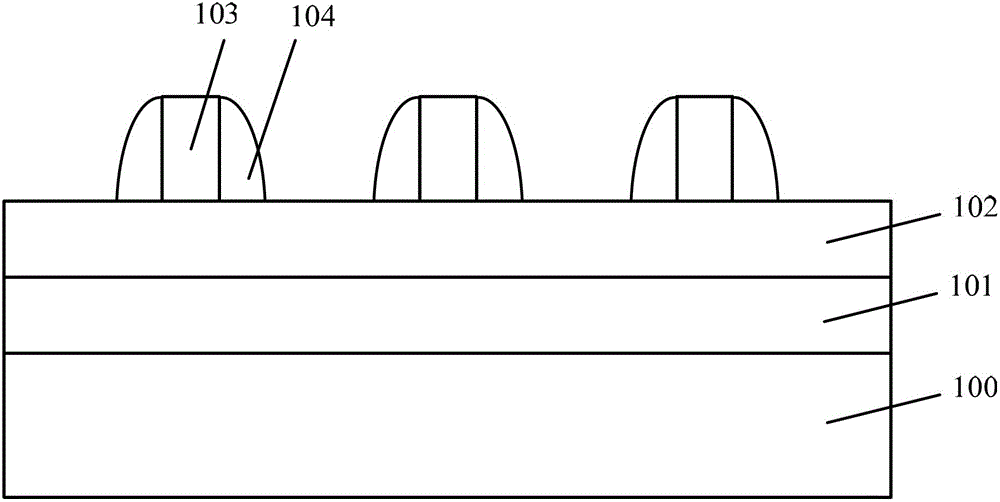
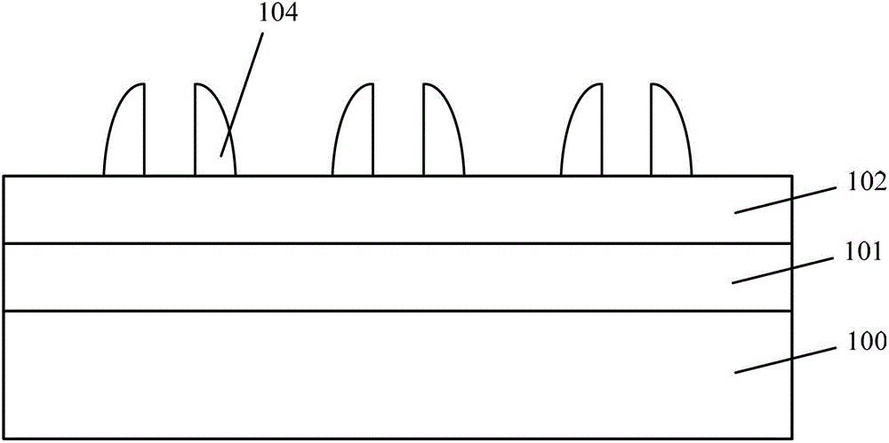
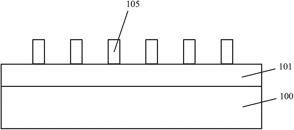
A forming method of a multigraph comprises the following steps: providing an etched material layer; forming a plurality of discrete first hard mask layers on the etched material layer; forming a first side wall positioned around the first hard mask layer; forming a second side wall positioned around the first side wall, and the first side wall and the second side wall are made of different materials; repeating the technology forming the first side wall and the second side wall for a plurality of times, and forming multi-layer side wall structures around the first hard mask layer spaced by the first side wall and the second side wall; removing the first hard mask layer and the second side wall; using the first side wall to serve as a mask so as to etch the etched material layer, thereby forming the target graph. In the forming method of the multigraph, the target graph is small in linewidth, the target graph with controllable number can be realized without carrying out hard mask transfer for many times, so technology is simple.

Description

technical field [0001] The invention relates to the technical field of semiconductors, in particular to a method for forming multiple patterns. Background technique [0002] With the continuous shrinking of the minimum line width and spacing of integrated circuit design, when the feature size of the exposure line is close to the theoretical resolution limit of the exposure system, the lithographic imaging will be severely distorted, resulting in a serious decline in the quality of the lithographic pattern. . In order to reduce the influence of the optical proximity effect, the industry has proposed a photolithographic resolution enhancement technology. [0003] One of the technologies is the double exposure (Double Print) technology, which uses multiple exposure technology to obtain a smaller line width, but the process of the double exposure technology is complicated, the cost is high, and there is alignment between multiple exposures (Alignment )question. [0004] Anoth...

Claims


Application Information

Patent Timeline
IPC IPC(8): H01L21/033
CPCH01L21/033H01L21/0338
Inventor 卜伟海康劲王文博
Owner SEMICON MFG INT (SHANGHAI) CORP
Why Eureka
Eureka Blog
Learn More