A Broadband Low Offset Active Balun Circuit
A circuit and broadband technology, applied in the field of active Balun circuits, can solve the problems of signal gain loss, large occupied area, difficult differential signal, small amplitude offset and phase offset, etc., to achieve small amplitude offset, small amplitude offset and phase offset, The effect of small phase misalignment
- Summary
- Abstract
- Description
- Claims
- Application Information
AI Technical Summary
Problems solved by technology
Method used
Image
Examples
Embodiment Construction
[0038] Take the design of an active Balun circuit with low amplitude offset and phase offset and wide frequency band input frequency between 24.25GHz and 26.65GHz as an example.
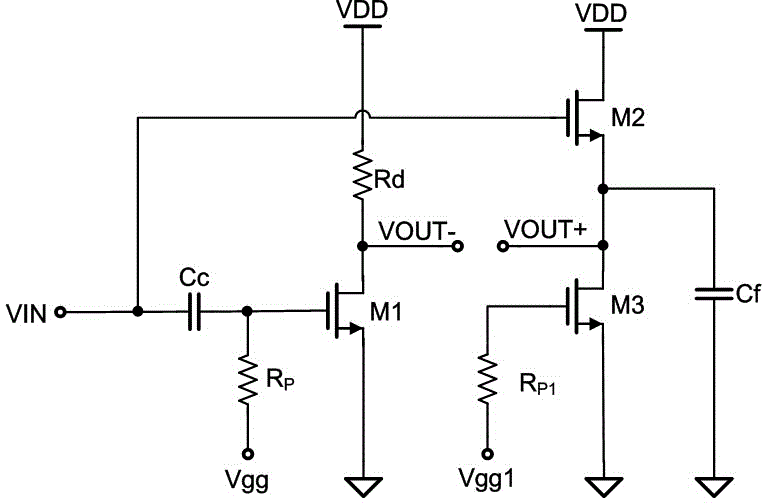
[0039] design circuit as figure 1 shown. The TSMC 0.13μm RF CMOS 1P8M process is adopted, the simulation tool is CadenceSpectreRF, and the power supply voltage is 1.2V. Where Vgg=Vgg1=620mV.
[0040] The MOS tubes are all radio frequency NMOS tubes, the resistors are high resistance polysilicon resistors, the capacitors are MIM capacitors, and the eighth layer of metal wiring.
[0041] When the input signal size is -40dBm signal, the amplitude offset of the active Balun in the wide frequency range of 24.25GHz~26.65GHz under layout PSS simulation is less than 0.16dB, and the phase offset is less than 0.9°; the static DC power consumption of the circuit is 2.8mW . The relationship between the differential signal amplitude offset and frequency can be obtained as Figure 4 As shown, while the relati...
PUM
 Abstract
Description
Claims
Application Information
 - R&D
- Intellectual Property
- Life Sciences
- Materials
- Tech Scout
- Unparalleled Data Quality
- Higher Quality Content
- 60% Fewer Hallucinations
Browse by: Latest US Patents, China's latest patents, Technical Efficacy Thesaurus, Application Domain, Technology Topic, Popular Technical Reports.
© 2025 PatSnap. All rights reserved.Legal|Privacy policy|Modern Slavery Act Transparency Statement|Sitemap|About US| Contact US: help@patsnap.com


