Transistor gate array with different lengths and fabrication method thereof
A manufacturing method and transistor technology, applied in semiconductor/solid-state device manufacturing, semiconductor devices, electrical components, etc., can solve the problem of limited time-consuming deviation, achieve the effect of reducing deviation, easy to implement, and not involving complicated calculations
- Summary
- Abstract
- Description
- Claims
- Application Information
AI Technical Summary
Problems solved by technology
Method used
Image

Examples
Embodiment 1
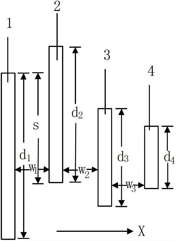
[0058] In the first embodiment, the fabrication method of the present invention is introduced by taking the target array, that is, the case where the lengths of the gates in the grid array to be formed are not equal, as an example. Specifically, such as figure 1 The target gate array with 4 gates is shown, the lengths of gates 1, 2, 3, 4 are d 1 、d 2 、d 3 、d 4 , which ranges, for example, from 0.03 microns to 3 microns. Among them, in the vertical gate length direction, that is, in the X direction, the lower end of the gate 1 in the array is the longest, and the upper end of the gate 2 is the longest, and the overlapping length of the two gates 1 and 2 in the length direction is s; The widths of poles 1, 2, 3, and 4 can be equal or unequal, and the distance between gate 1 and gate 2 is w 1 , the distance between gate 2 and gate 3 is w 2 , the distance between gate 3 and gate 4 is w 3 , where w 1 、w 2 、w 3 Can be equal or unequal. In one embodiment, the widths of the...
Embodiment 2
[0076] The second embodiment still introduces the manufacturing method of the present invention by taking the case that the lengths of the gates in the target array are not equal as an example. The difference from Embodiment 1 is that the target array has the longest gate, and the two ends of other gates in the target array do not exceed the two ends of the longest gate along the vertical gate length direction. Specifically, such as Figure 7 The target gate array with 4 gates is shown, where the length of gate 1 d 1 The longest, the two ends of the other gates 2, 3, 4 are along the vertical gate length direction, that is, the X direction, and do not exceed the two ends of the longest gate 1.
[0077] When using the first mask A' to expose the first photoresist 103 (positive photoresist) on the polysilicon 102 in step S12, as Figure 8 As shown, each light-shielding pattern ( Figure 8 The shaded area in ) is the length d of the longest gate 1 in the target array 1 . In o...
Embodiment 3
[0086] The transistor gate arrays with different lengths provided in the third embodiment and the manufacturing method thereof are substantially the same as those in the second embodiment. The difference is that the transistor gate target array has multiple sub-arrays, for example, as Figure 12 As shown, for sub-arrays 1', 2', 3', and 4', the target gate lengths of each sub-array are equal, and the target gate lengths of different sub-arrays are different, and each gate of sub-array 1' is the longest gate , the two ends of the gates of other sub-arrays in the target array do not exceed the two ends of the longest gate along the vertical gate length direction.
[0087] It can be understood that, during the execution of step S12, if Figure 13 As shown, when using the first mask A'' to expose the first photoresist 103 (positive photoresist) on the polysilicon 102, the light-shielding patterns of the first mask A'' ( Figure 13 The shaded area in ) corresponds to the gates of ...
PUM
 Abstract
Description
Claims
Application Information
 - R&D
- Intellectual Property
- Life Sciences
- Materials
- Tech Scout
- Unparalleled Data Quality
- Higher Quality Content
- 60% Fewer Hallucinations
Browse by: Latest US Patents, China's latest patents, Technical Efficacy Thesaurus, Application Domain, Technology Topic, Popular Technical Reports.
© 2025 PatSnap. All rights reserved.Legal|Privacy policy|Modern Slavery Act Transparency Statement|Sitemap|About US| Contact US: help@patsnap.com