Printed wiring board and manufacturing method thereof

A technology for printed circuit boards and wiring layers, which is applied in the fields of printed circuit manufacturing, printed circuits, printed circuits, etc. It can solve the problems of insulation resistance degradation, easy accumulation of moisture, and increased connection resistance of the insulating layer, so as to prevent solder bumps from interacting with each other. Inter-short circuit, insulation and connection reliability are excellent, and the effect of suppressing the deterioration of insulation resistance

Active Publication Date: 2010-06-16
IBIDEN CO LTD
View PDF4 Cites 0 Cited by
  • Summary
  • Abstract
  • Description
  • Claims
  • Application Information

AI Technical Summary

Problems solved by technology

[0006] Such an underfill material is filled and solidified to produce a printed wiring board for mounting an IC chip. However, when there are cavities in the cured underfill material, moisture is easily accumulated in the cavity, and the printed wiring board is subjected to high temperature. In the HAST test in a humid environment, based on the void existing at the interface between the surface of the solder resist layer and the underfill material, or near the interface between the underfill material and the IC, it is easy to get between the solder mask layer and the underfill material, or Cracks between underfill material and IC
Therefore, there is a problem that the insulation resistance of the insulating layer composed of the solder resist layer and the underfill material deteriorates, and peeling occurs between the substrates, thereby increasing the connection resistance between the IC chip and the solder bump.
[0007] In addition, there is a problem that moisture enters from the cracked interface, the solder migrates from the solder bumps, and the solder bumps are short-circuited between each other.

Method used


Image

  • Printed wiring board and manufacturing method thereof
  • Printed wiring board and manufacturing method thereof
  • Printed wiring board and manufacturing method thereof

Examples


Embodiment 1

[0106] Hereinafter, an example of the printed wiring board and its manufacturing method of the present invention will be described with reference to the drawings. First, refer to Figure 7 and Figure 8 The first embodiment of the printed wiring board of the present invention will be described.

[0107] Figure 7 Shows the cross section of the printed wiring board 10 (package substrate) before mounting the IC chip 90 as an electronic component, Figure 8 It shows the cross section of the printed wiring board 10 in the state which mounted the IC chip 90. Such as Figure 8 As shown, an IC chip 90 is mounted on the upper surface of the printed wiring board 10, and the lower surface is connected to the daughter board 94.

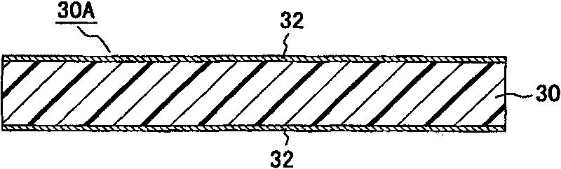
[0108] The printed wiring board 10 of this embodiment has a form in which build-up wiring layers 80A and 80B are formed on the front and back surfaces of the core substrate 30, respectively. The build-up wiring layer 80A is composed of an interlayer resin insulating...

Embodiment 2

[0177] The area of ​​the solder resist layer (electronic component mounting area) corresponding to the area (C4 area) where the conductor pads for IC chip mounting are provided is 70 mm 2 , And the number of conductor pads provided in the mounting area was 2000 (the same as the number of electrodes of the IC chip), except that the printed wiring board was manufactured in the same manner as in Example 1.

[0178] In addition, the surface in the electronic component mounting area in this embodiment is formed as an uneven surface with a maximum roughness of 0.5 μm.

Embodiment 3

[0180] The area of ​​the solder resist layer (electronic component mounting area) corresponding to the area (C4 area) where the conductor pad for IC chip mounting is provided is 130 mm 2 , And the number of conductor pads provided in the mounting area was 4000, except that the printed wiring board was manufactured in the same manner as in Example 1.

[0181] In addition, the surface in the electronic component mounting area in this embodiment is formed as an uneven surface with a maximum roughness of 0.4 μm.


PUM

PropertyMeasurementUnit
surface roughnessaaaaaaaaaa

Abstract

Disclosed is a printed wiring board wherein a solder resist layer is formed on the surface of a wiring board which is provided with a conductor circuit, a part of the conductor circuit exposed from anopening formed in the solder resist layer is formed into a conductor pad, a solder bump is formed on the conductor pad, an electronic component is mounted on the board via the solder bump, and the electronic component is sealed with an underfill resin. In this printed wiring board, the surface of the solder resist layer is planarized at least in the electronic component mounting region or the planarized surface is further subjected to a roughening treatment. Also disclosed is a method for manufacturing such a printed wiring board.

Description

Technical field [0001] The present invention relates to a printed wiring board used for packaging substrates for mounting electronic components such as ICs, and more particularly to a surface structure of a solder resist layer in which holes are not left in under-package materials such as ICs are sealed with resin. Background technique [0002] Picture 11 It shows a conventional printed wiring board constituting a package substrate. In the printed wiring board 210, a plurality of solder bumps 276 are formed on the substrate in order to mount the IC chip 290 or the like on the substrate, and a solder resist layer 270 is provided so that the solder bumps 276 are not welded to each other. [0003] Specifically, a conductor circuit 258 including a solder pad 275 is formed on the substrate, a solder resist layer 270 is provided to cover the conductor circuit 258, and an opening 271 is provided in the solder resist layer 270 at a position corresponding to the solder pad. After the nicke...

Claims


Application Information

Patent Timeline
Patent Type & Authority Patents(China)
IPC IPC(8): H01L23/12H05K3/28
CPCH01L2924/01088H05K3/381H01L2224/81801H01L2224/16H01L23/498H01L2924/01038H01L2924/15311H01L2224/13099H01L2924/01013H01L2224/32225H01L2924/0103H01L21/4846H01L2924/15174H01L24/81H01L2224/73204H01L23/49811H05K2203/0278H01L2924/01033H01L2924/01074H01L2924/01078H05K2201/10977H01L2224/16225H01L2224/85444H01L2224/8121H01L2924/01051H01L2924/01015H01L2924/01023H01L2924/01046H01L2924/01082H01L2224/16237H01L2924/01018H01L21/563H01L2924/01019H01L2924/01029H05K3/4602H01L2924/01027H01L24/11H05K2201/10674H01L2924/014H01L2924/01084H05K3/3452H05K3/305H01L2924/01047H05K3/3436H01L2924/01079H01L2224/81815H01L23/49827H01L24/16H01L2224/48227H01L2924/14H01L2924/01005H01L2924/01006H01L2224/81192H01L2924/01011H01L2924/01058H01L2224/0554H01L2224/05568H01L2224/05573H01L2924/00014H01L2924/12042Y10T29/49117Y10T29/49128Y10T29/49144Y10T29/49155Y10T428/2804Y10T428/31511Y10T428/31681Y02P70/50H01L2924/00H01L2224/05599H01L2224/0555H01L2224/0556
Inventor 川村洋一郎泽茂树丹野克彦田中宏德藤井直明
Owner IBIDEN CO LTD
Why Eureka
Try Eureka