Metallization method for back contact solar battery
A solar cell and back contact technology, applied in the field of solar cells, can solve the problems of limiting the advantages of back contact cells, increasing the cost of non-silicon processing of cells, and affecting the connection of components, so as to facilitate automatic welding of components, reduce non-silicon processing costs, and increase The effect of large welding area
- Summary
- Abstract
- Description
- Claims
- Application Information
AI Technical Summary
Problems solved by technology
Method used
Image
Examples
Embodiment 1
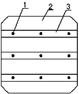
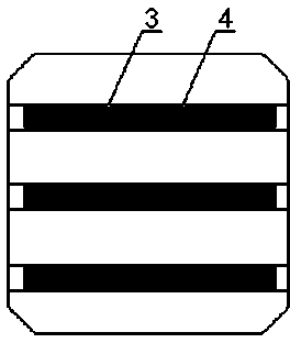
[0048] see Figure 1~4 Shown, a kind of MWT solar cell metallization manufacturing method comprises the steps:
[0049] (1) Clean the original silicon wafer, remove the damaged layer, and then form a suede surface;
[0050] (2) Put the above-mentioned silicon wafer into a diffusion furnace for phosphorus diffusion, and the front side of the silicon wafer is the diffusion surface;
[0051] (3) Remove the back parasitic junction and peripheral junction by chemical etching on the diffused silicon wafer;
[0052] (4) Deposit the SiNx layer on the front side of the silicon wafer;
[0053] (5) forming a series of symmetrically distributed small holes on the silicon wafer by laser; forming 3 rows and 3 columns in total;
[0054] (6) Print Ag metal dots at the hole position on the back of the silicon wafer to realize the contact between the metal dots and the semiconductor; obtain N-type metal contact 1;
[0055]The N-type metal contact is a circular point contact with a diameter o...
Embodiment 2
[0077] see Figure 5~9 Shown, a kind of IBC solar cell metallization manufacturing method comprises the steps:
[0078] (1) Forming N on the back side of the silicon wafer + Zone 5 and P + launch zone 6;
[0079] (2) Deposit Al on the back of the above silicon wafer 2 o 3 / SiN x laminated passivation layer;
[0080] (3) Deposit SiN on the front side of the silicon wafer x layer;
[0081] (4) On silicon wafer P + The emission area 6 is windowed by laser, and the windowed area accounts for P + 6% of the emission area;
[0082] (5) On wafer P + The Al paste 7 is screen-printed in the emission area, and the Al paste completely covers the area of the laser window;
[0083] (6) On the back of the wafer N + Print Ag paste 8 at the position of the area to realize the contact between the metal point and the semiconductor, and obtain the N-type metal contact;
[0084] The N-type metal contact is a circular point contact with a diameter of 0.5 mm;
[0085] (7) drying and...
PUM
| Property | Measurement | Unit |
|---|---|---|
| Thickness | aaaaa | aaaaa |
| Welding tension | aaaaa | aaaaa |
Abstract
Description
Claims
Application Information
 - R&D
- Intellectual Property
- Life Sciences
- Materials
- Tech Scout
- Unparalleled Data Quality
- Higher Quality Content
- 60% Fewer Hallucinations
Browse by: Latest US Patents, China's latest patents, Technical Efficacy Thesaurus, Application Domain, Technology Topic, Popular Technical Reports.
© 2025 PatSnap. All rights reserved.Legal|Privacy policy|Modern Slavery Act Transparency Statement|Sitemap|About US| Contact US: help@patsnap.com


