Wafer level packaging method and packaging structure for image sensor

A wafer-level packaging and image sensor technology, applied in radiation control devices, etc., can solve problems such as poor reliability of T-shaped connections, radiation damage to devices, and large capacitance values, and overcome poor reliability, small signal delay, and small capacitance. value effect

Inactive Publication Date: 2014-06-11
SHANGHAI INST OF MICROSYSTEM & INFORMATION TECH CHINESE ACAD OF SCI
View PDF3 Cites 10 Cited by
  • Summary
  • Abstract
  • Description
  • Claims
  • Application Information

AI Technical Summary

Problems solved by technology

[0006] In view of the shortcomings of the prior art described above, the object of the present invention is to provide a wafer-level packaging method and packaging structure for an image sensor, which is used to solve the problem of poor reliability of the T-type connection in the prior art and the high cost and high capacitance of the conventional TSV method. The problem of large value and radiation damage to the device

Method used


Image

  • Wafer level packaging method and packaging structure for image sensor
  • Wafer level packaging method and packaging structure for image sensor
  • Wafer level packaging method and packaging structure for image sensor

Examples


Embodiment

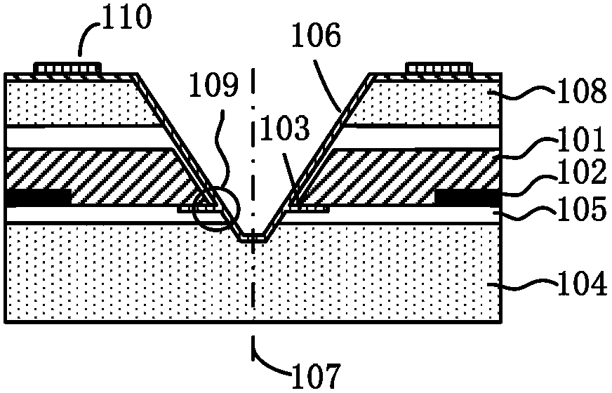
[0068] This embodiment provides a wafer-level packaging method for an image sensor, such as Figure 2a to Figure 2k As shown, the flow of this method is:

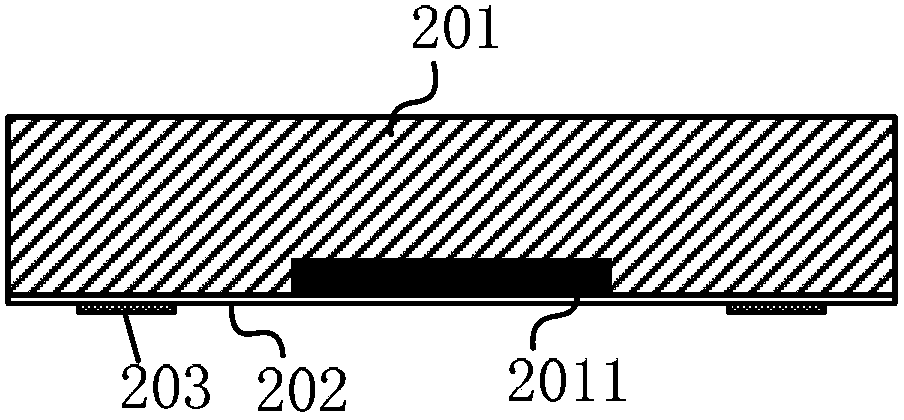
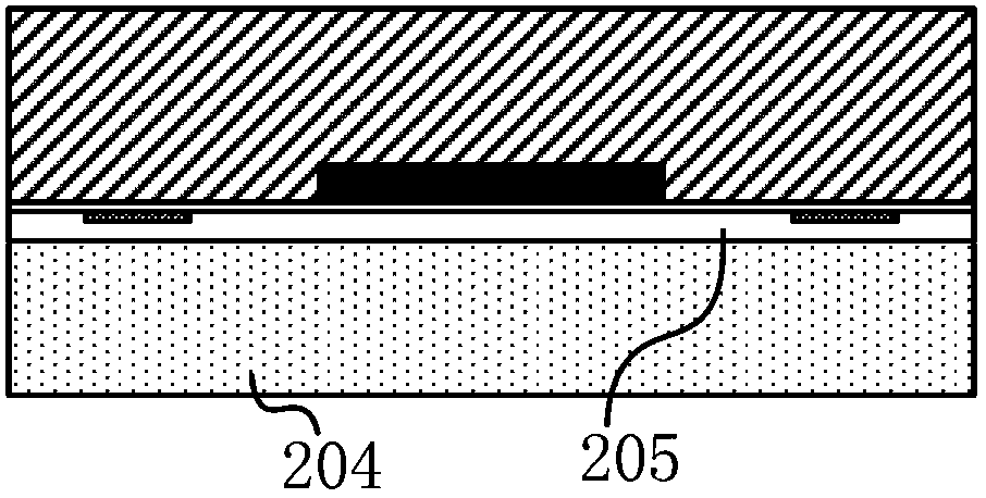
[0069] A) Fabricate a sensing wafer 201, and form a first passivation layer 202 on the active surface of the sensing wafer 201; wherein, the preset manufacturing process of the sensing wafer 201 includes: setting a Wafer; image sensing unit 2011 is formed on the front side of each chip; so far, the wafer constitutes a sensing wafer.

[0070] Specifically, the wavelength band used by the image sensing unit is in the visible light range, the standard thickness of the sensing wafer is preferably 350um, and the material of the sensing wafer is preferably gallium arsenide GaAs.

[0071] B) Depositing at least one metal fanning electrode 203 on the first passivation layer 202 ; the metal fanning electrode 203 is distributed around the image sensing unit 2011 .

[0072] Specifically, the metal fanning electrodes 203 are distribu...


PUM


Abstract

The invention provides a wafer level packaging method and packaging structure for an image sensor. The packaging method comprises the steps that a first passivation layer is formed on the active face of a sensing wafer; at least one metal fan-out electrode is deposited on the first passivation layer; the active face of the sensing wafer and a transparent substrate are bonded; a second passivation layer is deposited on the back face of the sensing wafer, and a grooving mark is carved on the second passivation layer; grooves are formed in the grooving mark; a third passivation layer is manufactured on the back face of the sensing wafer; through holes penetrating through the metal fan-out electrodes are formed in the bottoms of the grooves; metal interconnecting wires are manufactured to guide the metal fan-out electrodes out to the back face of the third passivation layer through the through holes; a fourth passivation layer completely covering the metal interconnecting wires is manufactured; an opening is etched in the fourth passivation layer to expose one ends of the metal interconnecting wires; a UBM layer and soldering tin protrusions are manufactured on the fourth passivation layer. The wafer level packaging method and packaging structure are high in reliability, low in cost, small in signal delay and high in interconnecting density.

Description

technical field [0001] The invention belongs to the technical field of image sensor packaging and manufacturing, and relates to a wafer-level packaging method and packaging structure of an image sensor. Background technique [0002] Generally speaking, an image sensor is a semiconductor module that converts an optical image into an electronic signal, and stores the image signal or transmits the image signal to a display device for display. With the trend of miniaturization and multi-function in the semiconductor industry and continuous competition in the market, a new generation of mobile products has higher requirements for image sensors, such as small form factor and low cost. The packaging of traditional image sensors adopts methods such as Chip On Board (COB for short) and Chip On Flexible (COF for short). The above packaging methods make it difficult for image sensors to meet today's demand. [0003] In order to solve the above problems, a wafer level packaging techno...

Claims


Application Information

Patent Timeline
Patent Type & Authority Applications(China)
IPC IPC(8): H01L27/146
Inventor 叶交托罗乐徐高卫王双福
Owner SHANGHAI INST OF MICROSYSTEM & INFORMATION TECH CHINESE ACAD OF SCI
Why Eureka
Try Eureka