Method of forming memory device

A storage device and dielectric layer technology, which is applied in the manufacture of electric solid-state devices, semiconductor devices, semiconductor/solid-state devices, etc., can solve problems such as poor memory performance, and achieve the effect of stable control circuits

Active Publication Date: 2016-07-06
SEMICON MFG INT (SHANGHAI) CORP
View PDF5 Cites 0 Cited by
  • Summary
  • Abstract
  • Description
  • Claims
  • Application Information

AI Technical Summary

Problems solved by technology

[0015] The problem solved by the present invention is that the performance of the storage device with nanocrystalline particle floating gate structure formed by the prior art is not good

Method used


Image

  • Method of forming memory device
  • Method of forming memory device
  • Method of forming memory device

Examples


Embodiment Construction

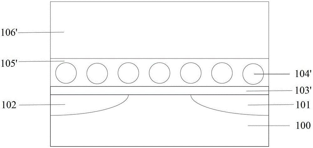
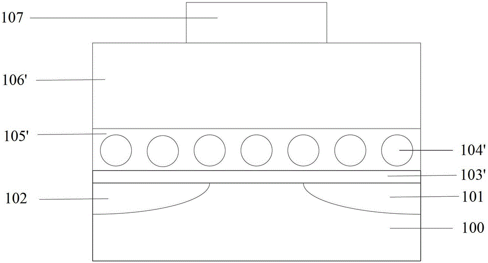
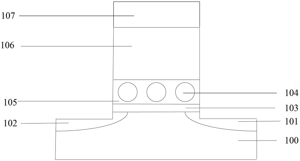
[0053] After research, the inventor found that the reason for the poor performance of the memory with the floating gate structure of nanocrystalline particles is:

[0054]When forming a traditional floating gate memory device, such as a SONOS memory, firstly a silicon oxide layer, a second polysilicon layer, an ONO dielectric layer and a first polysilicon layer are sequentially formed on a substrate. Next, a patterned mask layer is formed on the first polysilicon layer. Then, using the patterned hard mask as a mask, dry etching the first polysilicon layer, the ONO dielectric layer, the second polysilicon layer to the silicon oxide layer. Since the selectivity ratio of the second polysilicon layer to the silicon oxide layer is very high, it is easy to stop on the silicon oxide layer at the end of the dry etching process, thereby forming a control gate, an inter-gate dielectric layer, and a floating gate. However, in the first method of forming a storage device with a floating ...


PUM


Abstract

The invention provides a method for forming a storage device, comprising: providing a semiconductor substrate, on which a first dielectric layer with an opening is formed, a tunneling dielectric layer is provided at the bottom of the opening, and semiconductor layers on both sides of the opening Forming an active region and a drain region in the substrate; forming a floating gate on the tunnel dielectric layer, a second dielectric layer on the floating gate, and a gate on the second dielectric layer in the opening. control grid. The formation method of the storage device of the present invention can avoid over-etching the substrate, avoid leakage current, and improve the performance of the storage device.

Description

technical field [0001] The invention relates to the field of semiconductor manufacturing, in particular to a method for forming a memory device. Background technique [0002] Floating gate structure memory devices are currently widely used and generally recognized mainstream memory device types. They are very important semiconductor components and are widely used in the electronics and computer industries. Traditional floating gate memory devices, such as SONOS (Silicon-Oxide-Nitride-Oxide-Silicon, SONOS for short) memory, require fast write / erase operations and long-term high-stability storage due to their own structure and material selection. Conflicting limitations, and this contradiction has not been significantly improved with the shrinking of technology nodes, limit the development of floating gate memory devices. [0003] A memory device with a floating gate structure of nanocrystalline particles, which uses nanocrystalline particles as a charge storage medium, and e...

Claims


Application Information

Patent Timeline
Patent Type & Authority Patents(China)
IPC IPC(8): H01L21/8247H01L21/28
CPCH01L29/66825H01L29/66833H10B41/00H10B43/00
Inventor 何其旸洪中山隋运奇
Owner SEMICON MFG INT (SHANGHAI) CORP
Why Eureka
Try Eureka