Universal error-tolerant and error-correcting circuit and its applied decoder and triple-mode redundant circuit
An error correction circuit and decoder technology, applied in the field of integrated circuits, can solve problems such as lack of strong error correction capability and increased bit error rate
- Summary
- Abstract
- Description
- Claims
- Application Information
AI Technical Summary
Problems solved by technology
Method used
Image
Examples
Embodiment 1
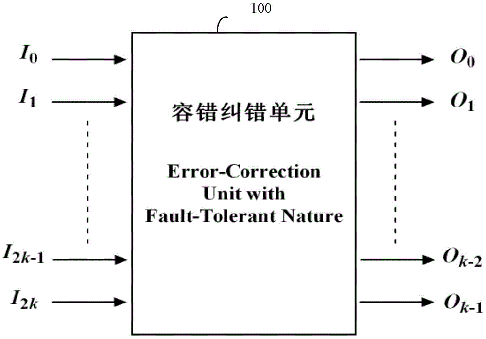
[0058] see figure 2 , which is a schematic structural diagram of a general error-tolerant and error-correcting circuit provided by the present invention.
[0059] The general error-tolerant and error-correcting circuit provided in this embodiment is characterized in that it includes: an error-tolerant and error-correcting unit 100 implemented by logic gates;
[0060] The digital input signals of the error-tolerant and error-correcting unit 100 are respectively I 0 , I 1 ..., I 2k-1 , I 2k ; The digital output signals of the error-tolerant and error-correcting unit are respectively O 0 , O 1 ...,O k-2 , O k-1 ; The digital input signal and the digital output signal belong to the set {0,1}; wherein, k is a positive integer;
[0061] The error-tolerant and error-correcting unit is used when k=1, if I 0 =I 1 , then O 0 =I 0 , otherwise O 0 =I 2 ; When k>1, if O k-2 =I 2k-1 , then O k-1 =I 2k-1 , otherwise O k-1 =I 2k .
[0062] In order to enable those skille...
Embodiment 2
[0078] see Figure 5 , which is a schematic diagram of Embodiment 2 of the error-tolerant and error-correcting circuit provided by the present invention.
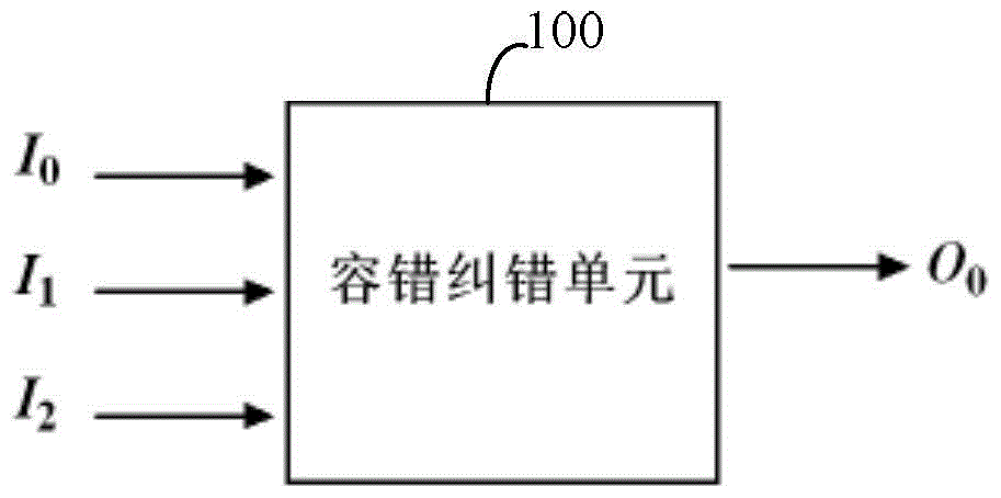
[0079] When k=1 in the error-tolerant and error-correcting unit provided by the present embodiment, the corresponding three digital input signals are respectively: I 0 , I 1 , I 2 ; Corresponding to a digital output signal: O 0 ;
[0080] The error-tolerant and error-correcting unit includes: a first AND gate A1, a first OR gate B1, a second AND gate A2, and a second OR gate B2;
[0081] The two input signals of the first OR gate B1 are respectively I 0 , I 1 ;
[0082] The two input signals of the first AND gate A1 are respectively I 0 , I 1 ;
[0083] An input signal I of the second AND gate A2 2 , the output signal of the first OR gate B1 is used as another input signal of the second AND gate A2;
[0084] The output signal of the second AND gate A2 and the output signal of the first AND gate A1 are used as tw...
Embodiment 3
[0088] Figure 5 Shown is the implementation of the circuit when k=1, combined below Figure 6 Introduce the circuit implementation when k=3.
[0089] see Figure 6 , which is a schematic diagram of Embodiment 3 of the error-tolerant and error-correcting circuit provided by the present invention.
[0090] In this embodiment, when k=3 in the error-tolerant and error-correcting unit, the corresponding seven digital input signals are respectively: I 0 , I 1 , I 2 , I 3 , I 4 , I 5 , I 6 ; Corresponding to three digital output signals are: O 0 , O 1 , O 2 ;
[0091]The error-tolerant and error-correcting unit includes three error-tolerant and error-correcting subunits, which are respectively the first error-tolerant and error-correcting subunit 100a, the second error-tolerant and error-correcting subunit 100b, and the third error-tolerant and error-correcting subunit 100c; each error-tolerant and error-correcting subunit Each unit corresponds to three digital input si...
PUM
 Abstract
Description
Claims
Application Information
 - R&D
- Intellectual Property
- Life Sciences
- Materials
- Tech Scout
- Unparalleled Data Quality
- Higher Quality Content
- 60% Fewer Hallucinations
Browse by: Latest US Patents, China's latest patents, Technical Efficacy Thesaurus, Application Domain, Technology Topic, Popular Technical Reports.
© 2025 PatSnap. All rights reserved.Legal|Privacy policy|Modern Slavery Act Transparency Statement|Sitemap|About US| Contact US: help@patsnap.com


