
SiC etching method for gentle and smooth side wall morphology

A smooth, topographic technology that can be used in electrical components, semiconductor/solid-state device manufacturing, circuits, etc., to solve problems such as narrowing of mask strip widths

Active Publication Date: 2014-04-09
STATE GRID CORP OF CHINA +1
View PDF5 Cites 8 Cited by
  • Summary
  • Abstract
  • Description
  • Claims
  • Application Information

AI Technical Summary

Problems solved by technology

[0004] In view of the deficiencies in the prior art, the purpose of the present invention is to provide a SiC etching method with gentle and smooth sidewall morphology. The present invention has changed the process of only using the wet etching mask layer in the past, thereby solving the problems caused by wet etching. The problem of narrowing the width of the mask stripes caused by side etching, this method can effectively and conveniently obtain the SiC etching morphology with smooth and smooth side walls

Method used


Image

  • SiC etching method for gentle and smooth side wall morphology
  • SiC etching method for gentle and smooth side wall morphology
  • SiC etching method for gentle and smooth side wall morphology

Examples


Embodiment 1

[0030] 1) Cleaning SiC material:

[0031] The SiC material 1 to be etched is sequentially subjected to the following cleaning steps:

[0032] 1# cleaning solution (ammonia: hydrogen peroxide: pure water = 1:1:5), temperature 70° for 5 minutes; 2# cleaning solution (hydrochloric acid: hydrogen peroxide: pure water = 1:1:5), temperature 70° for 5 minutes 1 minute; BOE cleaning solution (hydrofluoric acid: ammonium fluoride = 1:20), room temperature, time 30 seconds; acetone ultrasonic 5 minutes; isopropanol ultrasonic 5 minutes; DI water rinse 5 minutes, dry, and set aside.

[0033] 2) Deposit a loose mask layer:

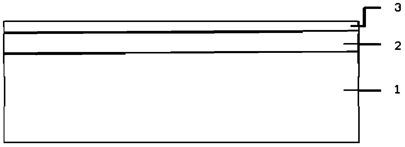
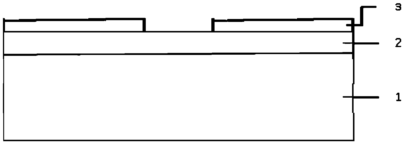
[0034] Using PECVD, namely plasma enhanced chemical vapor deposition method, room temperature deposition mask layer 2, its chemical composition is SiO2, see figure 1 . According to the thickness of the SiC material 1 to be etched 2um and the etching selectivity ratio 2, it is determined that the thickness of the mask layer 2 to be deposited is not less than 1um. Co...

Embodiment 2

[0050] 1) Cleaning SiC material:

[0051] The SiC material 1 to be etched is sequentially subjected to the following cleaning steps:

[0052] 1# Cleaning solution (ammonia: hydrogen peroxide: pure water = 1:1:5), temperature 70° for 5 minutes; BOE cleaning solution (hydrofluoric acid: ammonium fluoride = 1:20), room temperature, time 30 seconds; 2 #Cleaning solution (hydrochloric acid: hydrogen peroxide: pure water = 1:1:5), temperature 70° for 5 minutes; BOE cleaning solution (hydrofluoric acid: ammonium fluoride = 1:20), room temperature, time 30 seconds; isopropyl Alcohol ultrasonication for 5 minutes; acetone ultrasonication for 5 minutes; isopropanol ultrasonication for 5 minutes; DI water rinse for 5 minutes, dry and set aside.

[0053] 2) Deposit a loose mask layer:

[0054] Using ICPCVD, i.e. plasma enhanced chemical vapor deposition method, room temperature deposition mask layer 2, its chemical composition is SiON, see figure 1 . According to the thickness of the ...


PUM


Abstract

The invention relates to the manufacturing technology of SiC devices, in particular to a SiC etching method for gentle and smooth side wall morphology. The method includes the steps of cleaning SiC materials, depositing a loose mask layer, photoetching, carrying out dry etching on the mask layer, carrying out wet etching on a smooth mask layer, removing photoresist and carrying out dry etching on the SiC materials. The key process improvement refers to that dry etching on the loose mask layer and wet etching on the smooth mask layer are combined. According to the method, the process of only adopting wet etching on the mask layer is changed, and therefore the problem that the mask bar width is decreased due to lateral erosion in the wet etching is solved. By means of the method, the SiC etching morphology of gentle and smooth side walls can be obtained effectively and conveniently.

Description

technical field [0001] The invention relates to the manufacturing technology of SiC devices, in particular to a SiC etching method with gentle and smooth sidewall morphology. Background technique [0002] Semiconductor etching is not only a method of semiconductor surface processing, but also an important patterning method in the semiconductor device manufacturing process. [0003] In the etching of SiC materials, the high hardness and chemical stability of SiC materials can only be etched at high temperatures (about 1200 degrees Celsius). This high-temperature processing technology cannot meet the etching requirements in device manufacturing. The accuracy also causes great difficulties for the selection of etching mask materials. For this reason, the dry etching process is widely used to etch SiC materials. SiC etching method with gentle step morphology The dry etching process of SiC materials generally includes: SiC material cleaning, deposition of mask layer, photolithog...

Claims


Application Information

Patent Timeline
Patent Type & Authority Applications(China)
IPC IPC(8): H01L21/02
CPCH01L21/0445
Inventor 杨霏陆敏田亮张昭于坤山
Owner STATE GRID CORP OF CHINA
Learn More