Manufacturing method of array substrate, array substrate and display device

The technology of an array substrate and a manufacturing method, which is applied to the display field, can solve the problems of complex and cumbersome manufacturing process of the array substrate, low production efficiency, low economic benefit, etc., and achieves the effects of simple manufacturing steps, few manufacturing steps, and improved economic benefits.

Active Publication Date: 2014-04-02
BOE TECH GRP CO LTD
View PDF3 Cites 13 Cited by
  • Summary
  • Abstract
  • Description
  • Claims
  • Application Information

AI Technical Summary

Problems solved by technology

[0009] From the above, it can be seen that the manufacturing process of the array substrate of the existing multi-dimensional electric field display panel is complex and cumbersome, the production efficiency is low, the cost is high, and the economic benefit is low.

Method used


Image

  • Manufacturing method of array substrate, array substrate and display device
  • Manufacturing method of array substrate, array substrate and display device
  • Manufacturing method of array substrate, array substrate and display device

Examples


Embodiment Construction

[0049] The present invention will be further described below in conjunction with the accompanying drawings and embodiments.

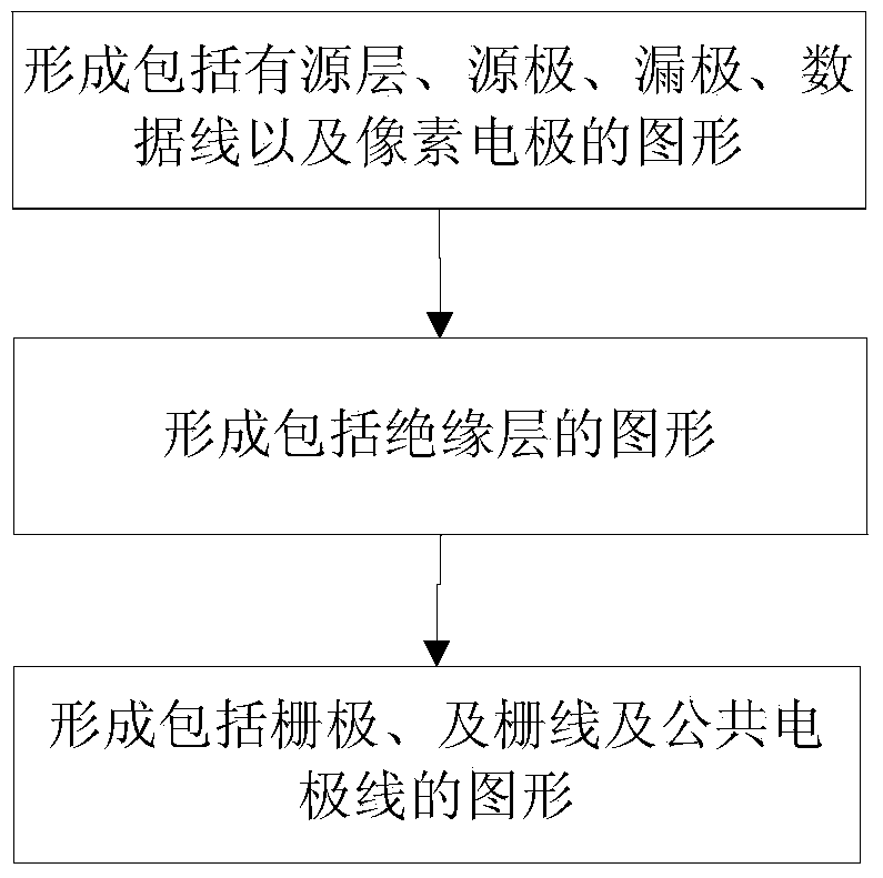
[0050] Such as figure 1 As shown, the fabrication method of the array substrate in this embodiment includes

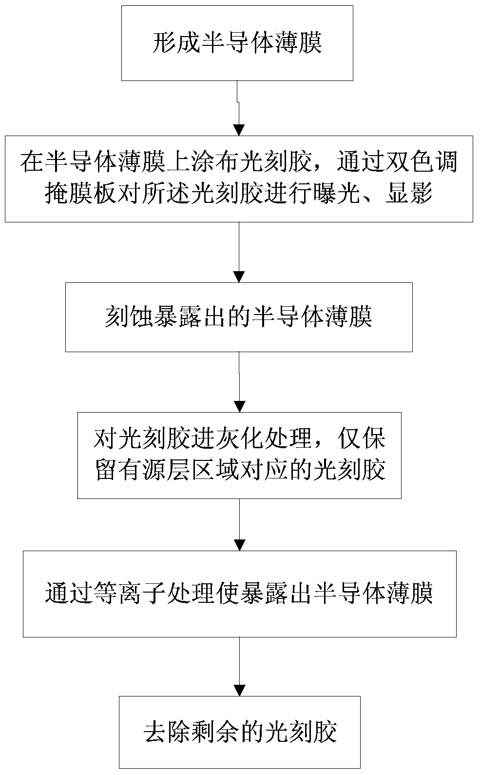
[0051] Step S1: forming a pattern including an active layer, a source electrode, a drain electrode, a data line, and a pixel electrode on the transparent substrate through a patterning process;

[0052] Step S2: forming a pattern including an insulating layer;

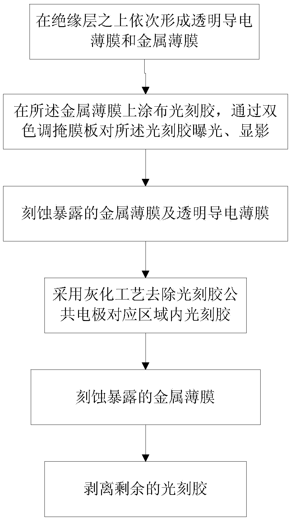
[0053] Step S3: forming a pattern including gates and gate lines through one patterning process.

[0054] In step S1, a pattern including an active layer, a source electrode, a drain electrode, a data line and a pixel electrode is formed through a patterning process;

[0055] In step S2, on the pattern formed in step S1, the pattern including the insulating layer is formed by depositing the insulating layer, wherein the deposition can be selected from any existing deposition method, a...


PUM


Abstract

The invention discloses a manufacturing method of an array substrate, the array substrate and a display device which are designed for solving the problems that an existing manufacturing technology of the array substrate is complicated, the economic benefit is low, and the like. The manufacturing method of the array device comprises the steps of forming a graph comprising an active layer, a source electrode, a drain electrode, a data line and a pixel electrode on a transparent substrate through one graph composition technology; forming a graph comprising an insulation layer; forming a graph comprising a grid electrode and a grid line through one graph composition technology. The manufacturing method of the array substrate, the array substrate and the display device, which are disclosed by the invention, have multiple advantages that the manufacturing technology is simple, the structure is simple and ingenious, the cost of a consumable device is low, the economic benefit is low, and the like.

Description

technical field [0001] The present invention relates to the field of display, in particular to a manufacturing method of an array substrate, an array substrate and a display device. Background technique [0002] The existing array substrates used for multi-dimensional electric field display panels need to go through 6-7 patterning processes in order to complete the fabrication of the array substrates. Each patterning process needs to go through the formation of the material to be etched, the coating, exposure and development of the photoresist, etching, and the removal of the photoresist. A common production method includes the following steps: [0003] The first patterning process: forming a pattern including common electrodes, common electrode lines, gates and gate lines; [0004] The second patterning process: forming an active layer; [0005] The third patterning process: forming via holes; [0006] The fourth patterning process: forming patterns including source and...

Claims


Application Information

Patent Timeline
IPC IPC(8): H01L21/77H01L27/12
CPCH01L27/1214H01L27/127H01L27/1288H10K59/123H10K59/1216H01L27/1225H01L27/124
Inventor 刘圣烈崔承镇金熙哲宋泳锡
Owner BOE TECH GRP CO LTD
Why Eureka
Try Eureka