Method for reducing cutting thickness of solar polycrystalline silicon chip

A polysilicon wafer, cutting thickness technology, applied in the direction of fine working equipment, stone processing equipment, manufacturing tools, etc., can solve the problems of insufficient tensile strength of cutting steel wire, lower silicon wafer pass rate, large steel wire cutting, etc., to achieve Good for cutting efficiency, high cutting efficiency and small cutting gap

Inactive Publication Date: 2014-04-02
JIANGSU ZHAOJING PHOTOELECTRIC TECH DEV
View PDF0 Cites 2 Cited by
  • Summary
  • Abstract
  • Description
  • Claims
  • Application Information

AI Technical Summary

Problems solved by technology

[0006] But if on the basis of the prior art, simply reduce the pitch of the guide wheel groove and reduce the diameter of the cutting steel wire, the tensile strength of the cutting steel wire is not enough. At the contact between the steel wire and the guide wheel, because the lower part of the cutting steel wire is not cooled by mortar, it is easy to rub and generate high temperature, which makes the steel wire have a temperature difference between the upper and lower sides, so that the steel wire is more likely to break. At the same time, due to the steel wire cutting If the resistance of the silicon wafer is too large, when the thickness of the silicon wafer is too small, the silicon wafer will be damaged, and the qualified rate of the silicon wafer will decrease.

Method used


Image

  • Method for reducing cutting thickness of solar polycrystalline silicon chip
  • Method for reducing cutting thickness of solar polycrystalline silicon chip
  • Method for reducing cutting thickness of solar polycrystalline silicon chip

Examples


specific Embodiment approach

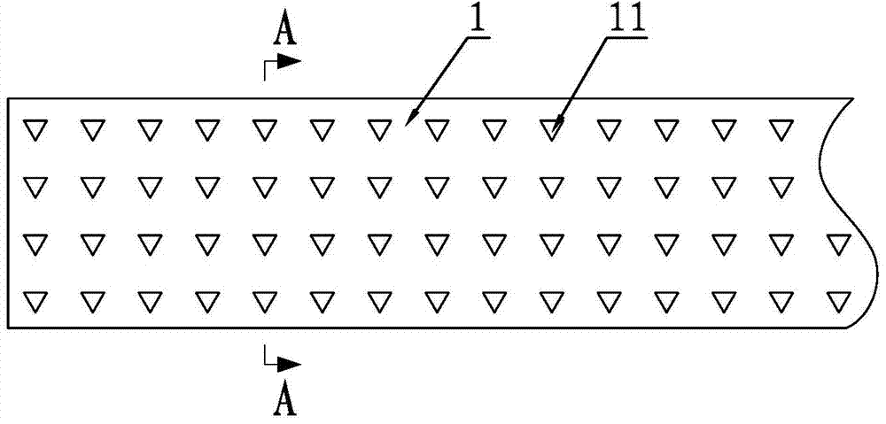
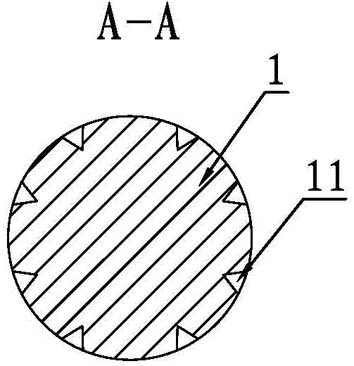
[0022] A method for reducing the cutting thickness of solar polysilicon wafers, such as Figure 1 to Figure 5 As shown, the cutting steel wire adopts a special-shaped cutting steel wire 1 with a diameter of 110-115 microns, the groove spacing of the guide wheel groove 21 on the guide wheel 2 is 320-330 microns, and the silicon carbide particles in the mortar have a particle size of 8.2-8.6 microns. The polygonal body, on the outer surface of the special-shaped cutting steel wire 1 is provided with a non-circular groove 11, the cross-sectional shape of the guide wheel groove 21 is isosceles trapezoidal, along the two sides of the guide wheel groove 21 The overflow grooves 22 are equidistantly arranged in the circumferential direction, the cross-sectional shape of the overflow grooves 22 is an isosceles trapezoid, the cross-sectional shape of the non-circular grooves 11 is triangular, and the non-circular grooves 11 are equidistantly arranged on the steel plate. On the outer sur...


PUM

PropertyMeasurementUnit
diameteraaaaaaaaaa
particle diameteraaaaaaaaaa

Abstract

The invention discloses a method for reducing the cutting thickness of a solar polycrystalline silicon chip. The structure of a guide wire groove is improved by adopting a small-diameter special cutting steel wire, the cutting steel wire can be cooled, the groove distance of the guide wire groove can be shortened, silicon carbide particles in mortar are polygon bodies of which the particle diameter is 8.2-8.6 mum, and the thickness of the solar silicon chip is reduced by mating three technical schemes. According to the method disclosed by the invention, not only can the thickness of the silicon chip be reduced, but also the processing accuracy of the silicon chip can be increased, the chip obtaining rate can be increased to a large extent, the cutting steel wire cannot rupture even the diameter of the cutting steel wire is small, the cutting efficiency is high, the cutting gap is small, the mortar using amount is less, the cutting loss of a silicon bar can be reduced, the chip obtaining rate can be increased, the production cost can be reduced, and the economic benefit is very significant.

Description

Technical field: [0001] The invention relates to polysilicon slicing technology, in particular to a method for reducing the cutting thickness of polysilicon solar cells. Background technique: [0002] Silicon is an important electronic and optical material, which plays an important role in a wide range of fields such as information, communication, aerospace, and environmental protection. The market demand is increasing, but the high price of solar cells affects the promotion of solar cells. The main factor of the application. Solar silicon wafers are the basic raw materials for solar cells. The low yield rate of solar silicon rods is the main reason for the high cost of silicon wafers. How to increase the yield rate of single crystal silicon rods or polycrystalline ingots is the most concerned by people. technical problem. At present, multi-wire cutting is generally used in the processing method of silicon wafers. Multi-wire cutting is to grind and cut the ingot through th...

Claims


Application Information

Patent Timeline
Patent Type & Authority Applications(China)
IPC IPC(8): B28D5/04
Inventor 王德明杨方谈军王庆峰陈远峰
Owner JIANGSU ZHAOJING PHOTOELECTRIC TECH DEV
Why Eureka
Try Eureka